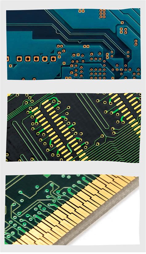
Introduction to PCB Fabrication
Printed Circuit Board (PCB) fabrication is a crucial process in the electronics industry. It involves the creation of a board that holds and connects electronic components to form a functional circuit. The quality and speed of PCB fabrication can greatly impact the success of an electronic product. In this article, we will explore the various aspects of fast and quality PCB fabrication.
The PCB Fabrication Process
The PCB fabrication process consists of several steps, each of which plays a critical role in the final quality of the board. These steps include:
- Design and Layout
- Material Selection
- Etching
- Drilling
- Plating
- Solder Mask Application
- Silkscreen Printing
- Surface Finish Application
- Electrical Testing
- Packaging and Shipping
Design and Layout
The first step in PCB fabrication is the design and layout of the circuit. This involves creating a schematic diagram of the circuit and then converting it into a physical layout using specialized software. The layout must take into account factors such as component placement, trace width and spacing, and power distribution.
Material Selection
The choice of materials for PCB fabrication is critical to the performance and reliability of the final product. The most common materials used for PCBs are:
| Material | Description |
|---|---|
| FR-4 | A composite material made of fiberglass and epoxy resin, known for its high strength and good electrical insulation properties. |
| Polyimide | A high-performance polymer material that can withstand extreme temperatures and has excellent electrical insulation properties. |
| Aluminum | Used for heat dissipation in high-power applications. |
| Copper | Used for the conductive layers of the PCB. |
Etching
Etching is the process of removing unwanted copper from the PCB to create the desired circuit pattern. There are two main methods of etching:
-
Chemical Etching: This method involves using a chemical solution to dissolve the unwanted copper. It is a slower process but can produce very fine features.
-
Plasma Etching: This method uses a plasma to remove the unwanted copper. It is a faster process but may not be suitable for very fine features.
Drilling
Drilling is the process of creating holes in the PCB for component leads and vias. The holes are typically drilled using a computer-controlled drill machine. The accuracy and precision of the drilling process are critical to the final quality of the PCB.
Plating
Plating is the process of coating the drilled holes and other exposed copper surfaces with a conductive material, typically copper. This ensures good electrical conductivity and prevents oxidation of the copper. There are two main types of plating:
-
Electroless Plating: This method involves immersing the PCB in a chemical solution that deposits a thin layer of copper on the surfaces.
-
Electrolytic Plating: This method involves applying an electric current to the PCB while it is immersed in a plating solution, resulting in a thicker layer of copper.
Solder Mask Application
Solder mask is a protective coating applied to the PCB to prevent solder from adhering to unwanted areas during the assembly process. It also provides insulation and protection against environmental factors such as moisture and dust.
Silkscreen Printing
Silkscreen printing is the process of applying text and symbols to the PCB for identification and assembly purposes. This is typically done using a stencil and a special ink that adheres to the solder mask.
Surface Finish Application
Surface finish is a protective coating applied to the exposed copper surfaces of the PCB to prevent oxidation and enhance solderability. There are several types of surface finishes, each with its own advantages and disadvantages:
| Surface Finish | Advantages | Disadvantages |
|---|---|---|
| HASL (Hot Air Solder Leveling) | Low cost, good solderability | Uneven surface, may cause thermal stress |
| ENIG (Electroless Nickel Immersion Gold) | Flat surface, good solderability, long shelf life | Higher cost, possible nickel corrosion |
| OSP (Organic Solderability Preservative) | Low cost, flat surface | Limited shelf life, may cause poor solderability |
| Immersion Silver | Low cost, good solderability | Limited shelf life, may tarnish over time |
| Immersion Tin | Low cost, good solderability | Limited shelf life, may cause whiskers |
Electrical Testing
Electrical testing is performed to ensure that the PCB functions as intended and meets the specified requirements. This may include continuity testing, insulation resistance testing, and functional testing.
Packaging and Shipping
Once the PCB has passed all the necessary tests, it is packaged and shipped to the customer. Proper packaging is essential to prevent damage during transit and ensure that the PCB arrives in good condition.

Factors Affecting PCB Fabrication Quality
Several factors can affect the quality of PCB fabrication, including:
-
Design and Layout: A poor design or layout can result in signal integrity issues, electromagnetic interference, and other problems.
-
Material Selection: Using low-quality or inappropriate materials can lead to reliability issues and reduced performance.
-
Manufacturing Processes: Improper or inconsistent manufacturing processes can result in defects such as shorts, opens, and poor solderability.
-
Environmental Factors: Exposure to moisture, dust, and other environmental factors can degrade the performance and reliability of the PCB.
-
Human Error: Mistakes made by operators during the fabrication process can lead to defects and quality issues.

Ensuring Fast and Quality PCB Fabrication
To ensure fast and quality PCB fabrication, it is essential to:
-
Use a reputable and experienced PCB manufacturer with a proven track record of quality and reliability.
-
Provide clear and accurate design files and specifications to the manufacturer.
-
Select appropriate materials and surface finishes based on the specific requirements of the application.
-
Implement strict quality control measures throughout the fabrication process, including inspections and testing at various stages.
-
Use automated manufacturing processes where possible to minimize human error and improve consistency.
-
Maintain good communication with the manufacturer throughout the fabrication process to address any issues or concerns promptly.

Conclusion
PCB fabrication is a complex process that requires careful attention to detail and strict quality control measures. By understanding the various aspects of PCB fabrication and working closely with a reputable manufacturer, it is possible to achieve fast and quality PCB fabrication that meets the specific requirements of the application.
Frequently Asked Questions (FAQ)
- What is the typical turnaround time for PCB fabrication?
-
The turnaround time for PCB fabrication can vary depending on the complexity of the design, the materials used, and the manufacturing processes involved. Typical turnaround times range from a few days to several weeks.
-
What is the minimum feature size that can be achieved with PCB fabrication?
-
The minimum feature size that can be achieved with PCB fabrication depends on the manufacturing processes used and the capabilities of the manufacturer. Typical minimum feature sizes range from 3 to 6 mils (0.003 to 0.006 inches) for standard PCBs, and can be as small as 1 mil (0.001 inches) for high-density interconnect (HDI) PCBs.
-
What is the difference between single-sided and double-sided PCBs?
-
Single-sided PCBs have conductive traces on only one side of the board, while double-sided PCBs have conductive traces on both sides of the board. Double-sided PCBs offer higher component density and better signal integrity than single-sided PCBs.
-
Can PCBs be fabricated with multiple layers?
-
Yes, PCBs can be fabricated with multiple layers, typically ranging from 2 to 12 layers or more. Multi-layer PCBs offer higher component density, better signal integrity, and improved power distribution compared to single-layer PCBs.
-
What is the typical cost of PCB fabrication?
- The cost of PCB fabrication can vary widely depending on factors such as the size and complexity of the board, the materials used, the manufacturing processes involved, and the quantity ordered. Typical costs range from a few dollars to several hundred dollars per board, with higher volumes generally resulting in lower per-unit costs.
Leave a Reply