What are square traces on a PCB?
Square traces, also known as rectangular traces, refer to the shape of the copper conductors used to route signals on a printed circuit board (PCB). Unlike traditional rounded traces, square traces have 90-degree angles and a rectangular cross-section.
Square traces offer several advantages over rounded traces in certain applications:
-
Increased current carrying capacity: The sharp corners of square traces allow for a greater cross-sectional area compared to rounded traces of the same width. This increased area enables square traces to carry more current without overheating.
-
Improved high-speed signal integrity: At high frequencies, current tends to flow along the edges of a conductor due to the skin effect. Square traces have more edge area than rounded traces, which can lead to better high-speed signal performance and reduced signal loss.
-
Enhanced manufacturing consistency: Square traces are easier to manufacture consistently because they have well-defined edges and corners. This consistency can lead to more predictable electrical characteristics and improved reliability.
When to use square traces on a PCB
Square traces are particularly beneficial in the following scenarios:
-
High-current applications: Power traces, such as those used for power distribution or high-current signals, can benefit from the increased current carrying capacity of square traces. This is especially true for traces that need to handle currents exceeding 1 amp.
-
High-speed digital signals: Square traces can improve signal integrity for high-speed digital signals, such as those found in high-speed memory interfaces, high-bandwidth data buses, or high-frequency clock signals. The increased edge area of square traces can help minimize signal distortion and attenuation.
-
Controlled impedance traces: When designing controlled impedance traces, such as those used for differential pairs or transmission lines, square traces can provide more consistent and predictable impedance characteristics. This is due to the well-defined geometry of square traces, which allows for more accurate impedance calculations and simulations.
Designing with square traces on a PCB
When incorporating square traces into your PCB design, consider the following guidelines:
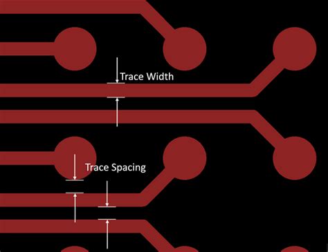
Trace width and spacing
The width and spacing of square traces should be carefully chosen based on the electrical requirements of your design. Factors to consider include:
- Current carrying capacity
- Impedance requirements
- Manufacturing constraints
- PCB layer stack-up
Use PCB design tools and calculators to determine the appropriate trace width and spacing for your specific application.
Routing considerations
When routing square traces, keep these points in mind:
-
Corners and angles: While square traces have 90-degree angles, it’s essential to avoid sharp corners in your routing. Sharp corners can cause signal reflections and create areas of high current density, leading to increased heat generation. Use chamfered or rounded corners to mitigate these issues.
-
Trace length matching: For high-speed signals or differential pairs, ensure that the length of the traces is carefully matched to maintain signal integrity and minimize skew. PCB design tools often include length matching features to assist with this process.
-
Impedance discontinuities: Pay attention to impedance discontinuities caused by changes in trace geometry, such as width changes or layer transitions. These discontinuities can cause signal reflections and degrade signal quality. Use impedance matching techniques, such as tapered transitions or stitching vias, to minimize these effects.
Manufacturing considerations
When designing with square traces, it’s crucial to communicate your requirements clearly with your PCB manufacturer. Ensure that your manufacturer is capable of producing square traces with the desired dimensions and tolerances. Some manufacturers may have limitations on the minimum trace width or spacing they can achieve with square traces.
Additionally, consider the impact of square traces on the overall manufacturability of your PCB. Square traces may require more precise etching and plating processes, which can increase manufacturing costs or lead times. Discuss these factors with your manufacturer to ensure that your design is feasible and cost-effective.

Examples of square traces on PCBs
Square traces can be found in various applications across different industries. Some examples include:
-
Power electronics: High-current power converters, such as those used in switched-mode power supplies or motor controllers, often employ square traces for their power distribution networks. The increased current carrying capacity of square traces helps to minimize power losses and improve overall efficiency.
-
High-speed digital interfaces: High-bandwidth memory interfaces, such as DDR4 or GDDR6, utilize square traces to maintain signal integrity and minimize signal loss at high frequencies. Square traces are also common in high-speed serial interfaces, such as PCIe or USB 3.0, where maintaining consistent impedance is critical.
-
RF and microwave circuits: In radio frequency (RF) and microwave applications, square traces are often used for controlled impedance transmission lines, such as microstrip or stripline. The well-defined geometry of square traces allows for accurate impedance matching and minimizes signal reflections.

FAQ
Q1: Can I mix square and rounded traces on the same PCB?
A1: Yes, it is possible to use both square and rounded traces on the same PCB. However, it’s essential to consider the transition points between the different trace geometries. Ensure that any changes in trace shape are gradual and well-controlled to minimize impedance discontinuities and signal reflections.
Q2: Are there any disadvantages to using square traces?
A2: One potential disadvantage of square traces is the increased manufacturing complexity compared to rounded traces. Square traces require more precise etching and plating processes, which can increase manufacturing costs or lead times. Additionally, square traces may be more susceptible to high-frequency losses due to skin effect, especially at extremely high frequencies.
Q3: How do I determine the appropriate trace width for my square traces?
A3: The appropriate trace width for square traces depends on several factors, including the current carrying requirements, impedance targets, and manufacturing constraints. Use PCB design tools and calculators, such as those provided by your PCB design software or online resources, to determine the optimal trace width for your specific application.
Q4: Can I use square traces for low-speed signals?
A4: While square traces offer benefits for high-speed and high-current applications, they can also be used for low-speed signals. However, the advantages of square traces may be less significant in low-speed applications, and traditional rounded traces may be sufficient.
Q5: How do I communicate my square trace requirements to my PCB manufacturer?
A5: When communicating your square trace requirements to your PCB manufacturer, provide clear and detailed information about the desired trace dimensions, tolerances, and any specific manufacturing constraints. Include this information in your PCB design files, fabrication drawings, and any accompanying documentation. Engage in a dialogue with your manufacturer to ensure that they can meet your requirements and to discuss any potential issues or limitations.

Conclusion
Square traces on PCBs offer several advantages over traditional rounded traces, particularly in high-current and high-speed applications. By providing increased current carrying capacity and improved signal integrity, square traces can enhance the performance and reliability of your PCB design.
When designing with square traces, carefully consider factors such as trace width, spacing, routing, and manufacturing constraints. Engage with your PCB manufacturer to ensure that your design is feasible and cost-effective.
By understanding the benefits and design considerations of square traces, you can leverage this technique to optimize your PCB designs and meet the ever-increasing demands of modern electronics.
Leave a Reply