Introduction to PCB Component Placement
Printed Circuit Board (PCB) component placement is a crucial step in the PCB assembly process. It involves the precise positioning and orientation of electronic components onto the PCB substrate. The placement process is guided by the PCB design, which specifies the location, orientation, and type of each component. Proper component placement is essential for ensuring the functionality, reliability, and manufacturability of the PCB.
Importance of PCB Component Placement
PCB component placement plays a vital role in the overall performance and quality of the PCB. Here are some key reasons why component placement is important:
-
Functionality: Proper component placement ensures that the PCB functions as intended. It allows for correct electrical connections and signal integrity between components.
-
Manufacturability: Efficient component placement facilitates the PCB assembly process. It considers factors such as component spacing, orientation, and accessibility for automated pick-and-place machines and manual soldering.
-
Reliability: Optimal component placement helps in reducing the risk of manufacturing defects and improves the reliability of the PCB. It minimizes the chances of short circuits, solder bridges, and component damage during assembly.
-
Thermal Management: Component placement takes into account the thermal characteristics of the components. Proper placement allows for adequate heat dissipation and prevents thermal stress on the PCB.
-
Signal Integrity: The placement of components, especially high-speed and sensitive components, affects signal integrity. Proper placement minimizes signal interference, crosstalk, and electromagnetic compatibility (EMC) issues.
PCB Component Placement Process
The PCB component placement process involves several steps to ensure accurate and efficient placement of components onto the PCB substrate. Here’s an overview of the typical component placement process:
1. PCB Design Review
Before starting the component placement, it is essential to review the PCB design. The design should be checked for accuracy, completeness, and adherence to design guidelines. Any issues or discrepancies in the design should be addressed and resolved prior to placement.
2. Component Preparation
The components required for the PCB assembly are prepared for placement. This includes:
- Inspection: Components are visually inspected for any damage, defects, or incorrect packaging.
- Kitting: Components are sorted and grouped according to the bill of materials (BOM) and placement requirements.
- Preform Preparation: If required, component leads are preformed or cut to the appropriate length for placement.
3. Solder Paste Stencil Printing
Before placing the components, solder paste is applied to the PCB pads using a stencil printing process. The stencil is aligned with the PCB, and solder paste is deposited onto the pads through the stencil openings. This process ensures precise and consistent solder paste application.
4. Automated Pick-and-Place
For high-volume production and surface mount components, automated pick-and-place machines are used for component placement. These machines use computer-controlled robotics to pick up components from feeders and place them accurately onto the PCB pads. The placement process is guided by the PCB design data, which specifies the location and orientation of each component.
5. Manual Placement
For through-hole components or low-volume production, manual placement may be performed. Skilled operators place the components onto the PCB by hand, following the placement instructions provided by the PCB design. Manual placement requires precision and attention to detail to ensure accurate positioning of the components.
6. Inspection and Verification
After component placement, a visual inspection is performed to verify the accuracy and completeness of the placement. Automated optical inspection (AOI) systems or manual inspection methods are used to check for any misaligned, missing, or incorrect components. If any issues are identified, they are corrected before proceeding to the soldering stage.

Component Placement Techniques
There are various techniques used for component placement onto PCBs. The choice of technique depends on factors such as the component type, package size, and production volume. Here are some common component placement techniques:
Surface Mount Technology (SMT)
Surface Mount Technology (SMT) is widely used for placing surface mount devices (SMDs) onto PCBs. SMDs are components that have small leads or terminations that are soldered directly onto the surface of the PCB pads. SMT placement is typically performed using automated pick-and-place machines, which offer high speed and accuracy.
SMT Placement Process
The SMT placement process involves the following steps:
- Solder Paste Printing: Solder paste is applied to the PCB pads using a stencil printing process.
- Component Placement: SMDs are picked up from feeders and placed onto the PCB pads by the pick-and-place machine.
- Reflow Soldering: The PCB with placed components undergoes a reflow soldering process, where the solder paste melts and forms a permanent connection between the components and the PCB pads.
Advantages of SMT Placement
SMT placement offers several advantages, including:
- High placement speed and accuracy
- Ability to place small and high-density components
- Reduced PCB size and weight
- Improved electrical performance
Through-Hole Technology (THT)
Through-Hole Technology (THT) involves placing components with long leads that are inserted into holes drilled in the PCB. The leads are then soldered to the PCB pads on the opposite side of the board. THT placement is commonly used for larger components or those that require higher mechanical strength.
THT Placement Process
The THT placement process involves the following steps:
- Component Insertion: THT components are manually inserted into the designated holes on the PCB.
- Lead Clinching: The component leads are bent or clinched to hold the components in place temporarily.
- Wave Soldering: The PCB undergoes a wave soldering process, where the bottom side of the board is exposed to a wave of molten solder. The solder adheres to the component leads and PCB pads, forming a permanent connection.
Advantages of THT Placement
THT placement offers certain advantages, such as:
- Higher mechanical strength and stability for larger components
- Ability to handle higher power components
- Easier manual assembly and rework
Mixed Technology Placement
Mixed technology placement involves the use of both SMT and THT components on the same PCB. This approach combines the benefits of both technologies and allows for greater flexibility in component selection and placement.
In mixed technology placement, SMDs are typically placed first using automated pick-and-place machines, followed by the manual insertion of THT components. The PCB then undergoes a combination of reflow soldering for SMDs and wave soldering for THT components.

Component Placement Guidelines
To ensure optimal PCB component placement, there are several guidelines and best practices to follow. These guidelines help in achieving reliable and manufacturable PCB assembly. Here are some key component placement guidelines:
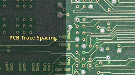
1. Component Spacing
Adequate spacing should be maintained between components to facilitate assembly and prevent short circuits. The spacing requirements depend on factors such as component size, package type, and soldering method. Industry standards and manufacturer recommendations provide guidance on minimum spacing requirements.
2. Orientation and Polarity
Components should be placed with the correct orientation and polarity as specified in the PCB design. Incorrect orientation or polarity can lead to functional issues and even component damage. Clear markings or indicators on the PCB and components help in ensuring correct placement.
3. Thermal Considerations
Components that generate significant heat should be placed in a manner that allows for proper heat dissipation. Adequate spacing and thermal management techniques, such as heatsinks or thermal vias, should be considered for high-power components. Thermal analysis can be performed to optimize component placement for effective heat distribution.
4. Signal Integrity
The placement of high-speed and sensitive components should be optimized to minimize signal integrity issues. Critical components should be placed close to their associated circuitry to reduce signal path lengths and minimize interference. Proper grounding and shielding techniques should be employed to mitigate electromagnetic compatibility (EMC) concerns.
5. Manufacturing Constraints
Component placement should consider manufacturing constraints such as component accessibility, soldering methods, and automated assembly capabilities. Components should be placed in a way that allows for efficient and reliable soldering processes. Clearance should be provided for automated pick-and-place nozzles and soldering equipment.
6. Testability and Rework
Component placement should facilitate testing and rework processes. Test points and probe access should be provided for critical components and signals. Components should be placed in a manner that allows for easy rework or replacement if needed, without damaging adjacent components.

PCB Component Placement Tools and Software
To aid in the PCB component placement process, various tools and software solutions are available. These tools provide automation, optimization, and visualization capabilities to streamline the placement process. Here are some commonly used PCB component placement tools and software:
1. CAD/CAM Software
Computer-Aided Design (CAD) and Computer-Aided Manufacturing (CAM) software are used for designing and generating PCB layouts. These software tools provide features for component placement, routing, and generation of manufacturing files. Popular CAD/CAM software for PCB design include:
- Altium Designer
- Cadence Allegro
- Mentor Graphics PADS
- KiCad
- Eagle
2. Placement Optimization Tools
Placement optimization tools are specialized software that automatically optimize component placement based on predefined constraints and design rules. These tools consider factors such as component spacing, signal integrity, and thermal management to generate an optimized placement layout. Some placement optimization tools include:
- Cadence Allegro PCB Placement Solution
- Mentor Graphics Valor NPI
- Siemens PCB Placement Automation
3. DFM Analysis Tools
Design for Manufacturability (DFM) analysis tools analyze the PCB design and component placement to identify potential manufacturing issues. These tools perform checks for design rule violations, component clearances, and solderability. DFM analysis helps in identifying and resolving placement-related issues early in the design process. Examples of DFM analysis tools include:
- Mentor Graphics Valor NPI
- Cadence PCB Design for Manufacturing (DFM)
- Zuken DFM Center
Challenges in PCB Component Placement
Despite advancements in tools and techniques, PCB component placement still presents challenges that need to be addressed. Here are some common challenges encountered in PCB component placement:
1. High-Density Designs
As electronic devices become more compact and feature-rich, PCB designs are becoming increasingly dense. Placing a large number of components in a limited space poses challenges in terms of component spacing, signal integrity, and thermal management. Advanced placement techniques and optimization tools are required to handle high-density designs effectively.
2. Miniaturization of Components
The trend towards miniaturization of electronic components presents challenges in component handling and placement. Small components, such as chip-scale packages (CSPs) and micro-BGAs, require precise placement and specialized equipment. Ensuring accurate placement and solderability of miniaturized components is crucial for reliable PCB assembly.
3. Mixed Technology Placement
Incorporating both SMT and THT components on the same PCB adds complexity to the placement process. Balancing the placement requirements of different component types and managing the transition between SMT and THT placement stages can be challenging. Careful planning and consideration of manufacturing constraints are necessary for successful mixed technology placement.
4. Thermal Management
With the increasing power density of modern electronic components, thermal management becomes a critical consideration in PCB component placement. Proper placement of high-power components and the use of thermal management techniques, such as heatsinks and thermal vias, are essential to prevent overheating and ensure reliable operation. Thermal analysis and simulation tools can assist in optimizing component placement for effective heat dissipation.
5. Signal Integrity and EMC
Maintaining signal integrity and managing electromagnetic compatibility (EMC) is a challenge in PCB component placement, especially for high-speed designs. Proper placement of sensitive components, such as clocks, transceivers, and RF modules, is crucial to minimize crosstalk, interference, and signal distortion. Careful consideration of signal routing, grounding, and shielding techniques is necessary to ensure optimal signal integrity and EMC performance.
Best Practices for PCB Component Placement
To overcome the challenges and ensure successful PCB component placement, following best practices is essential. Here are some key best practices for PCB component placement:
1. Collaborate with PCB Design and Manufacturing Teams
Close collaboration between PCB design and manufacturing teams is crucial for optimal component placement. Designers should consider manufacturing constraints and guidelines during the placement process. Manufacturing engineers should provide feedback and suggestions to optimize placement for manufacturability and reliability.
2. Use Automated Placement Tools
Utilizing automated placement tools and software can significantly improve the efficiency and accuracy of the placement process. These tools can optimize component placement based on predefined rules and constraints, reducing manual effort and minimizing the risk of placement errors.
3. Perform DFM Analysis
Conducting Design for Manufacturability (DFM) analysis helps identify and resolve placement-related issues early in the design process. DFM analysis tools can detect design rule violations, component clearance issues, and potential manufacturing challenges. Addressing these issues during the placement stage can save time and cost in the later stages of PCB assembly.
4. Adhere to Industry Standards and Guidelines
Following industry standards and guidelines for PCB component placement ensures consistency and reliability. Standards such as IPC (Association Connecting Electronics Industries) provide guidelines for component spacing, orientation, and soldering requirements. Adhering to these standards helps in achieving manufacturing compatibility and quality.
5. Conduct Thorough Testing and Inspection
Thorough testing and inspection of the placed components are essential to ensure the quality and reliability of the PCB assembly. Visual inspection, automated optical inspection (AOI), and electrical testing should be performed to detect any placement defects or issues. Catching and correcting placement errors early in the assembly process can save time and cost in the long run.
Conclusion
PCB component placement is a critical step in the PCB assembly process that directly impacts the functionality, reliability, and manufacturability of the PCB. Proper placement of components ensures correct electrical connections, signal integrity, and thermal management. The placement process involves various techniques, such as SMT and THT placement, and is guided by PCB design data and placement guidelines.
To achieve optimal component placement, it is essential to consider factors such as component spacing, orientation, thermal considerations, signal integrity, and manufacturing constraints. Utilizing automated placement tools, performing DFM analysis, and following industry standards and best practices can help overcome placement challenges and ensure successful PCB assembly.
As PCB designs continue to become more complex and dense, advancements in placement technologies and techniques will be crucial to keep pace with the evolving requirements of the electronics industry. By understanding the principles and best practices of PCB component placement, designers and manufacturers can collaborate effectively to create reliable and high-quality PCBs that meet the demands of modern electronic devices.
Frequently Asked Questions (FAQ)
1. What is PCB component placement?
PCB component placement is the process of positioning and orienting electronic components onto the PCB substrate according to the PCB design. It involves the precise placement of components onto the designated pads or through-holes on the PCB.
2. Why is proper component placement important in PCB assembly?
Proper component placement is crucial for ensuring the functionality, reliability, and manufacturability of the PCB. It allows for correct electrical connections, signal integrity, and thermal management. Misplaced or improperly oriented components can lead to functional issues, manufacturing defects, and reliability problems.
3. What are the different techniques used for PCB component placement?
The two main techniques used for PCB component placement are Surface Mount Technology (SMT) and Through-Hole Technology (THT). SMT involves placing surface mount devices (SMDs) onto the surface of the PCB pads, while THT involves inserting component leads through holes drilled in the PCB and soldering them on the opposite side.
4. What are some common challenges faced in PCB component placement?
Some common challenges in PCB component placement include high-density designs, miniaturization of components, mixed technology placement (combining SMT and THT), thermal management, and signal integrity issues. These challenges require careful consideration of placement guidelines, manufacturing constraints, and the use of advanced placement techniques and tools.
5. How can automated placement tools and software assist in the PCB component placement process?
Automated placement tools and software provide automation, optimization, and visualization capabilities to streamline the placement process. They can optimize component placement based on predefined constraints and design rules, considering factors such as component spacing, signal integrity, and thermal management. These tools help in improving placement accuracy, efficiency, and reducing the risk of placement errors.
| Characteristic | Surface Mount Technology (SMT) | Through-Hole Technology (THT) |
|---|---|---|
| Component Type | Surface Mount Devices (SMDs) | Through-Hole Components |
| Placement Method | Automated pick-and-place machines | Manual insertion |
| Soldering Process | Reflow soldering | Wave soldering |
| PCB Size and Density | Allows for smaller PCB sizes and higher component density | Requires larger PCB sizes and lower component density |
| Mechanical Strength | Lower mechanical strength compared to THT | Higher mechanical strength and stability |
| Manufacturing Speed | High-speed automated placement | Slower manual placement process |
| Rework and Repair | More challenging due to small component sizes | Easier manual rework and repair |
| Cost | Generally lower cost for high-volume production | Higher cost due to manual labor and larger PCB sizes |
Leave a Reply