What is PCB Impedance and Why Does it Matter?
PCB impedance refers to the opposition to alternating current in a printed circuit board (PCB). It is an important electrical characteristic that needs to be tightly controlled, especially in high-speed digital systems. Improper PCB impedance can lead to signal integrity issues, electromagnetic interference (EMI), and even complete system failure.
In high-speed digital designs, the traces on a PCB act as transmission lines. The characteristic impedance of these traces must match the impedance of the source and load to prevent reflections and ensure clean signal transmission. Any impedance mismatches can cause a portion of the signal to be reflected back to the source, leading to signal distortion, ringing, and other problems.
Moreover, uncontrolled impedance can cause crosstalk between adjacent traces, where a signal on one trace induces unwanted voltage on another. This can lead to false triggering, data corruption, and EMI issues.
Therefore, PCB impedance control is crucial for maintaining signal integrity, minimizing EMI, and ensuring reliable system performance. It involves careful design and manufacturing techniques to achieve the desired impedance values for PCB traces.
Factors Affecting PCB Impedance
Several factors influence the impedance of a PCB trace:
-
Trace geometry: The width, thickness, and spacing of the traces affect their impedance. Wider and thicker traces have lower impedance, while narrower and thinner traces have higher impedance.
-
Dielectric constant: The dielectric constant (Dk) of the PCB substrate material impacts the impedance. Higher Dk materials result in lower impedance traces.
-
Dielectric thickness: The thickness of the dielectric layer between the trace and the reference plane (usually ground or power plane) affects impedance. Thicker dielectrics lead to higher impedance.
-
Copper thickness: The thickness of the copper traces influences their impedance. Thicker copper results in lower impedance.
-
Frequency: The frequency of the signal affects the effective impedance of the traces. At higher frequencies, the impedance tends to decrease due to the skin effect and dielectric losses.

Types of PCB Impedance
There are two main types of PCB impedance:
-
Characteristic impedance (Z0): This is the impedance of a trace when it is infinitely long and perfectly matched. It depends on the trace geometry, dielectric constant, and dielectric thickness. The most common characteristic impedance values are 50Ω and 100Ω.
-
Differential impedance (Zdiff): This is the impedance between two traces carrying differential signals (e.g., USB, HDMI, Ethernet). It depends on the spacing between the traces, their geometry, and the dielectric properties. Differential impedance is typically around 90Ω to 120Ω.

Calculating PCB Impedance
To calculate the characteristic impedance of a PCB trace, you can use the following formulas:
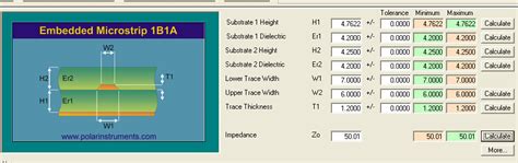
For microstrip (trace on the outer layer):
Z0 = 87 / √(ϵr + 1.41) × ln(5.98 × h / (0.8 × w + t))
For stripline (trace embedded between two reference planes):
Z0 = 60 / √ϵr × ln(1.9 × (2 × h) / (0.8 × w + t))
Where:
– Z0 is the characteristic impedance in ohms (Ω)
– ϵr is the dielectric constant of the substrate material
– h is the dielectric thickness in mils (1 mil = 0.001 inch)
– w is the trace width in mils
– t is the trace thickness (copper thickness) in mils
For differential impedance, you can use the following formula:
Zdiff = 2 × Z0 × (1 - 0.48 × e^(-0.96 × s / h))
Where:
– Zdiff is the differential impedance in ohms (Ω)
– Z0 is the characteristic impedance of a single trace (calculated using the microstrip or stripline formula)
– s is the edge-to-edge spacing between the differential traces in mils
– h is the dielectric thickness in mils
Here’s an example calculation for a microstrip trace with the following parameters:
– ϵr = 4.5
– h = 8 mils
– w = 10 mils
– t = 1.4 mils
Using the microstrip formula:
Z0 = 87 / √(4.5 + 1.41) × ln(5.98 × 8 / (0.8 × 10 + 1.4))
   = 87 / √5.91 × ln(48.384 / 9.52)
   = 87 / 2.431 × ln(5.082)
   = 35.786 × 1.625
   ≈ 58.15Ω
So, the characteristic impedance of this microstrip trace is approximately 58.15Ω.

PCB Impedance Control Techniques
To achieve the desired impedance values and maintain signal integrity, several PCB impedance control techniques can be employed:
-
Trace width and spacing control: Adjusting the width and spacing of the traces is the primary method for controlling impedance. Wider traces and larger spacing decrease impedance, while narrower traces and smaller spacing increase impedance.
-
Dielectric thickness control: Varying the thickness of the dielectric layer between the trace and the reference plane can help achieve the target impedance. Thicker dielectrics increase impedance, while thinner dielectrics decrease it.
-
Dielectric material selection: Choosing a PCB substrate material with the appropriate dielectric constant (Dk) is important for impedance control. Lower Dk materials result in higher impedance traces, while higher Dk materials lead to lower impedance.
-
Copper thickness control: The thickness of the copper traces can be adjusted to fine-tune the impedance. Thicker copper reduces impedance, while thinner copper increases it.
-
Reference plane placement: Proper placement of reference planes (ground or power) is crucial for impedance control. The reference plane should be as close to the signal layer as possible to minimize the dielectric thickness and maintain a consistent impedance.
-
Impedance matching: When a trace encounters a change in impedance (e.g., connector, via, or component), impedance matching techniques can be used to minimize reflections. This can involve adding series or parallel termination resistors, using impedance matching stubs, or designing tapered transitions.
-
Differential routing: For differential signals, it’s important to route the traces as a tightly coupled pair with controlled spacing. This helps maintain the differential impedance and minimizes crosstalk.
-
Via control: Vias can introduce impedance discontinuities and cause reflections. To minimize their impact, techniques such as via stitching, back drilling, and optimized via placement can be used.
-
Simulation and modeling: Before fabricating the PCB, it’s essential to simulate and model the impedance of critical traces using electronic design automation (EDA) tools. This helps identify and correct any impedance issues early in the design process.
PCB Impedance Measurement and Verification
After fabricating the PCB, it’s crucial to measure and verify the actual impedance values to ensure they match the design targets. There are several methods for measuring PCB impedance:
-
Time Domain Reflectometry (TDR): TDR is the most common method for measuring PCB impedance. It involves sending a fast-rise-time pulse down the trace and measuring the reflected signal. The shape and timing of the reflection provide information about the impedance profile along the trace.
-
Frequency Domain Reflectometry (FDR): FDR is similar to TDR but uses a swept frequency signal instead of a pulse. It measures the reflected signal at different frequencies to determine the impedance profile.
-
Vector Network Analyzer (VNA): A VNA can measure the S-parameters of a PCB trace, which can be used to calculate the impedance. It provides accurate results but requires a more complex setup compared to TDR or FDR.
-
Impedance Test Coupons: PCB manufacturers often include impedance test coupons on the production panel. These coupons have traces with known geometries and can be measured to verify the impedance of the actual PCB traces.
When measuring PCB impedance, it’s important to use proper techniques and equipment:
- Use high-quality, calibrated test equipment (TDR, VNA, etc.) to ensure accurate measurements
- Properly terminate the trace under test to avoid reflections from the far end
- Use a low-loss, high-bandwidth cable and probes to connect the test equipment to the PCB
- Minimize the probe loading effect by using probes with high input impedance and small capacitance
- Perform measurements in a controlled environment (temperature, humidity) to avoid variations
If the measured impedance values deviate significantly from the design targets, it may be necessary to modify the PCB design and repeat the fabrication and testing process. In some cases, post-fabrication techniques such as trace trimming or adding external components can be used to correct minor impedance issues.
Best Practices for PCB Impedance Control
To ensure successful PCB impedance control, follow these best practices:
-
Define impedance requirements early: Clearly specify the target impedance values and tolerances for each critical trace in the PCB design requirements document.
-
Use appropriate design rules: Establish design rules for trace width, spacing, and dielectric thickness based on the impedance requirements and the PCB fabrication capabilities.
-
Minimize impedance discontinuities: Avoid abrupt changes in trace width, spacing, or dielectric thickness, as they can cause impedance discontinuities and reflections.
-
Provide accurate PCB Stackup information: Clearly communicate the PCB stackup, including layer thicknesses, dielectric constants, and copper weights, to the PCB manufacturer to ensure accurate impedance control.
-
Perform pre-layout simulation: Use EDA tools to simulate the impedance of critical traces before finalizing the PCB layout. This helps identify and correct any impedance issues early in the design process.
-
Follow good layout practices: Route critical traces away from board edges, keep them straight and avoid unnecessary bends, and provide adequate spacing from other signals and components to minimize crosstalk.
-
Use ground planes: Place ground planes adjacent to critical signal layers to provide a stable reference and minimize impedance variations.
-
Specify controlled impedance in fabrication notes: Clearly indicate which traces require impedance control in the PCB fabrication notes, along with the target impedance values and tolerances.
-
Verify impedance on prototypes: Measure and verify the impedance of critical traces on prototype PCBs before proceeding with mass production.
-
Monitor impedance during production: Regularly measure and monitor the impedance of production PCBs to ensure consistency and catch any process variations.
Common PCB Impedance Control Challenges and Solutions
PCB impedance control can present several challenges, but most of them can be overcome with proper design and manufacturing techniques. Here are some common challenges and their solutions:
-
Impedance variations due to manufacturing tolerances: PCB fabrication processes have inherent tolerances that can cause impedance variations. To mitigate this, specify tighter tolerances for critical parameters (e.g., dielectric thickness, trace width) and work closely with the PCB manufacturer to ensure they can meet the requirements.
-
High-speed signal integrity issues: As signal speeds increase, maintaining impedance control becomes more challenging. To address this, use advanced PCB materials with lower loss tangents, employ differential signaling techniques, and carefully design the PCB stackup and layout to minimize discontinuities and crosstalk.
-
Limited board space: In dense PCB designs, it can be challenging to route traces with the desired impedance due to space constraints. To overcome this, use smaller trace widths and spacing, employ higher layer counts, and prioritize impedance control for the most critical signals.
-
Cost constraints: Achieving tight impedance control can increase PCB fabrication costs due to the need for more precise processes and materials. To balance cost and performance, prioritize impedance control for the most critical signals and use standard impedance values (e.g., 50Ω, 100Ω) whenever possible.
-
Impedance matching at connectors: Connectors can introduce impedance discontinuities that cause reflections and degrade signal integrity. To mitigate this, use connectors with a known impedance (e.g., 50Ω), design the PCB layout to minimize the stub length, and consider using impedance matching techniques (e.g., series termination resistors).
-
Impedance control in flex circuits: Flexible PCBs present unique challenges for impedance control due to their varying dielectric thickness and mechanical stress. To address this, use materials with stable dielectric properties, employ strain relief techniques, and consider using controlled-impedance flex cables.
-
Simulation accuracy: Impedance simulation results may not always match the actual PCB measurements due to modeling approximations and manufacturing variations. To improve simulation accuracy, use accurate PCB material properties, include the effects of copper roughness and plating, and correlate simulation results with measurements from test coupons.
PCB Impedance Control FAQ
-
Q: What is the difference between characteristic impedance and differential impedance?
A: Characteristic impedance (Z0) is the impedance of a single trace with respect to a reference plane, while differential impedance (Zdiff) is the impedance between two traces carrying differential signals. Differential impedance is typically higher than characteristic impedance and requires careful control of the spacing between the traces. -
Q: How does the dielectric constant affect PCB impedance?
A: The dielectric constant (Dk) of the PCB substrate material influences the impedance of the traces. Higher Dk materials result in lower impedance traces, while lower Dk materials lead to higher impedance traces. Therefore, the choice of dielectric material is an important factor in PCB impedance control. -
Q: What is the purpose of impedance matching in PCB design?
A: Impedance matching is used to minimize reflections and ensure clean signal transmission when a signal encounters a change in impedance, such as at a connector, via, or component interface. Techniques such as series or parallel termination resistors, impedance matching stubs, or tapered transitions can be employed to match the impedance and prevent signal degradation. -
Q: How can I specify impedance requirements to a PCB manufacturer?
A: To specify impedance requirements, include the following information in your PCB fabrication notes: - Target characteristic and/or differential impedance values and tolerances for each critical trace
- PCB stackup details, including layer thicknesses, dielectric constants, and copper weights
- Trace geometry requirements, such as width, spacing, and copper thickness
-
Any specific materials or processes needed for impedance control
-
Q: What are some common impedance values used in PCB design?
A: Some common characteristic impedance values used in PCB design are: - 50Ω: Commonly used for single-ended signals, such as coaxial cables and RF circuits
- 75Ω: Used in video and cable television applications
- 100Ω: Used in Ethernet and other high-speed digital applications
For differential impedance, common values range from 90Ω to 120Ω, depending on the specific interface standard (e.g., USB, HDMI, PCIe).
Conclusion
PCB impedance control is a critical aspect of high-speed digital design, ensuring signal integrity, minimizing EMI, and maintaining reliable system performance. By understanding the factors affecting PCB impedance, employing appropriate design and manufacturing techniques, and following best practices, designers can effectively control impedance and achieve optimal results.
Key points to remember:
- PCB impedance is the opposition to alternating current in a trace and must be controlled to prevent reflections and crosstalk
- Factors such as trace geometry, dielectric properties, and frequency influence PCB impedance
- Characteristic impedance (Z0) and differential impedance (Zdiff) are the two main types of PCB impedance
- Techniques such as trace width and spacing control, dielectric thickness adjustment, and reference plane placement can be used to control impedance
- PCB impedance can be measured using methods like TDR, FDR, and VNA, and should be verified on prototypes and production boards
- Best practices include defining impedance requirements early, using appropriate design rules, minimizing discontinuities, and closely collaborating with PCB manufacturers
By mastering PCB impedance control, designers can create high-performance, reliable electronic systems that meet the ever-increasing demands of modern applications.
Leave a Reply