What is BGA?
BGA, or Ball Grid Array, is a type of surface-mount packaging used for integrated circuits (ICs) that utilizes a grid of solder balls as the means of connection between the IC package and the printed circuit board (PCB). This advanced packaging technology has gained significant popularity in the electronics industry due to its numerous advantages over traditional packaging methods, such as enhanced electrical performance, reduced package size, and improved thermal management.
Advantages of BGA Packaging
- High interconnect density
- Excellent electrical performance
- Reduced package size
- Improved thermal management
- Enhanced reliability
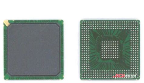
BGA Package Structure
A typical BGA package consists of several key components:
- Die: The semiconductor chip or integrated circuit.
- Substrate: A thin, multi-layered board that provides electrical connections between the die and the solder balls.
- Wire bonds or flip-chip bumps: Interconnects that link the die to the substrate.
- Solder balls: The array of small solder spheres that form the connection between the package and the PCB.
- Encapsulant or molding compound: A protective material that covers and safeguards the die and wire bonds.
BGA Substrate Materials
BGA substrates can be made from various materials, each with its own set of characteristics and benefits:
| Material | Characteristics | Typical Applications |
|---|---|---|
| FR-4 | Low cost, good electrical properties, adequate thermal performance | Consumer electronics, telecommunications |
| BT (Bismaleimide Triazine) | Higher glass transition temperature (Tg), better thermal performance than FR-4 | Automotive, aerospace, high-performance computing |
| Polyimide | Excellent thermal stability, high Tg, low dielectric constant | Military, aerospace, high-reliability applications |
| Ceramic | Outstanding thermal conductivity, high reliability, stable dielectric properties | High-power RF devices, high-temperature applications |

BGA Design Considerations
When designing a BGA package or integrating it into a PCB, several key factors must be considered to ensure optimal performance and reliability:
1. Ball Pitch and Size
The ball pitch, or the distance between the centers of adjacent solder balls, is a crucial parameter in BGA design. Common pitches range from 0.5mm to 1.27mm, with smaller pitches enabling higher interconnect density but also requiring more advanced PCB manufacturing capabilities. The size of the solder balls also affects the package’s performance and reliability.
2. Thermal Management
BGAs generate significant amounts of heat due to their high interconnect density. Effective thermal management is essential to prevent overheating and ensure reliable operation. This can be achieved through the use of thermal vias, heat spreaders, or heat sinks.
3. Signal Integrity
The high-speed nature of many BGA applications necessitates careful consideration of signal integrity. Factors such as impedance matching, crosstalk, and signal reflections must be addressed through proper PCB layout and design techniques, such as controlled impedance routing and ground plane management.
4. PCB Layout and Routing
Designing a PCB to accommodate a BGA package requires adherence to specific layout guidelines to ensure manufacturability, reliability, and optimal performance. This includes proper pad sizing and spacing, solder mask design, and via placement. The routing of traces to and from the BGA should also follow best practices to minimize signal integrity issues and maintain adequate clearances.

BGA Assembly Process
The assembly of a BGA package onto a PCB involves several critical steps:
- Solder Paste Application: Solder paste is applied to the PCB pads using a stencil or screen printing process.
- Component Placement: The BGA package is precisely placed onto the PCB using automated pick-and-place equipment.
- Reflow Soldering: The assembly is subjected to a controlled heating process in a reflow oven, causing the solder paste to melt and form reliable connections between the package and the PCB.
- Inspection: The assembled board undergoes visual and automated optical inspection (AOI) to verify the quality of the solder joints and detect any defects.
- Rework (if necessary): If defects are found, rework may be required, which involves the removal and replacement of the BGA package using specialized equipment.

BGA Testing and Quality Assurance
To ensure the reliability and performance of BGA assemblies, various testing and quality assurance methods are employed:
1. X-Ray Inspection
X-ray imaging is used to inspect the solder joints beneath the BGA package, which are not visible through conventional optical inspection methods. This allows for the detection of voids, bridging, or other defects that could compromise the assembly’s reliability.
2. Boundary Scan Testing
Boundary scan, or JTAG testing, is a method that uses built-in test circuitry within the BGA device to verify the interconnections between the package and the PCB. This enables the detection of opens, shorts, or other faults in the assembly.
3. Thermal Cycling
Thermal cycling tests expose the BGA assembly to alternating high and low-temperature extremes to simulate the stresses encountered during real-world operation. This helps to identify potential reliability issues related to thermal expansion mismatches or solder joint fatigue.
4. Microsectioning
Microsectioning involves cross-sectioning the BGA assembly and examining the solder joints under a microscope. This destructive testing method provides detailed information about the quality and structure of the solder joints, aiding in the identification of potential failure mechanisms.
Frequently Asked Questions (FAQ)
1. What are the primary advantages of BGA packaging over other package types?
BGA packaging offers several advantages, including higher interconnect density, improved electrical performance, reduced package size, better thermal management, and enhanced reliability compared to other package types such as Quad Flat Packages (QFPs) or Thin Small Outline Packages (TSOPs).
2. Can BGA packages be reworked if a defect is found during assembly?
Yes, BGA packages can be reworked using specialized equipment that allows for the removal and replacement of the package without damaging the PCB or surrounding components. However, rework can be challenging and time-consuming, making it essential to minimize the need for rework through careful design and process control.
3. How does the ball pitch affect the manufacturing process and PCB design?
Smaller ball pitches enable higher interconnect density but also require more advanced PCB manufacturing capabilities and stricter design rules. As the pitch decreases, the PCB layout becomes more complex, requiring tighter tolerances for pad sizing, spacing, and via placement. Smaller pitches also necessitate more precise solder paste application and component placement during assembly.
4. What are the key considerations for thermal management in BGA assemblies?
Effective thermal management is crucial for BGA assemblies due to their high interconnect density and the resulting heat generation. Key considerations include the use of thermal vias to transfer heat from the package to the PCB, the incorporation of heat spreaders or heat sinks to dissipate heat, and the selection of PCB materials with appropriate thermal conductivity.
5. How can signal integrity issues be addressed in BGA designs?
Signal integrity issues in BGA designs can be addressed through proper PCB layout and design techniques. This includes controlled impedance routing to minimize reflections and maintain signal quality, ground plane management to provide a low-impedance return path, and the use of simulation tools to analyze and optimize the design. Additionally, selecting appropriate substrate materials and minimizing the package’s internal inductance can help to mitigate signal integrity problems.
Conclusion
BGA packaging has revolutionized the electronics industry by enabling the development of smaller, faster, and more reliable electronic devices. By understanding the fundamentals of BGA technology, including its structure, design considerations, assembly process, and testing methods, engineers, and manufacturers can successfully integrate this advanced packaging solution into their products. As electronic systems continue to evolve and demand higher performance, BGA packaging will remain a critical tool in meeting these challenges and driving innovation forward.
Leave a Reply