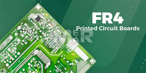
What is FR4 PCB?
FR4 (Flame Retardant 4) is a composite material consisting of woven fiberglass cloth impregnated with an epoxy resin binder. The “FR” stands for flame retardant, indicating its ability to self-extinguish and resist the spread of flames. FR4 is the most common base material used for manufacturing PCBs due to its superior properties and cost-effectiveness compared to other materials.
Properties of FR4 PCB
FR4 PCBs exhibit several desirable properties that make them suitable for a wide range of applications:
-
Electrical Insulation: FR4 has excellent electrical insulation properties, with a dielectric constant of approximately 4.5 at 1 MHz and a dielectric strength of about 20 kV/mm.
-
Mechanical Strength: The combination of fiberglass and epoxy resin provides FR4 with high mechanical strength and durability. It can withstand moderate impacts and vibrations without cracking or breaking.
-
Thermal Stability: FR4 maintains its structural integrity and properties over a wide temperature range, typically from -55°C to +125°C. It has a glass transition temperature (Tg) of around 130°C to 140°C.
-
Flame Retardancy: As the name suggests, FR4 is flame retardant. It self-extinguishes within seconds after the ignition source is removed, minimizing the risk of fire hazards.
-
Moisture Resistance: FR4 has low moisture absorption, making it suitable for use in humid environments. However, prolonged exposure to high humidity can still affect its properties.
FR4 PCB Manufacturing Process
The manufacturing process of FR4 PCBs involves several steps, each of which plays a crucial role in ensuring the quality and reliability of the final product. Let’s take a closer look at each step:
1. Material Preparation
The first step in FR4 PCB manufacturing is preparing the raw materials. The FR4 substrate is cut to the desired size and shape using precision cutting machines. The copper foil, which will form the conductive traces on the PCB, is also cut to size and cleaned to remove any contaminants.
2. Lamination
The next step is lamination, where the FR4 substrate and copper foil are bonded together using heat and pressure. The copper foil is placed on top of the FR4 substrate, and they are sandwiched between two metal plates. The stack is then placed in a lamination press, where it is subjected to high temperature (usually around 180°C) and pressure (around 300 psi) for a specific duration. This process ensures a strong and uniform bond between the FR4 and copper foil.
3. Drilling
After lamination, the PCB panels are drilled to create holes for through-hole components and vias. The drilling process is performed using high-speed CNC drilling machines equipped with carbide or diamond-tipped drill bits. The drill file, generated from the PCB design software, guides the machine to drill holes at precise locations on the panel.
4. Plating
Once the holes are drilled, the PCB undergoes a plating process to make the holes conductive and to form the copper traces on the surface. There are two common plating methods:
a. Electroless Plating: In this process, the PCB is immersed in a chemical bath containing a copper solution. The copper ions are reduced and deposited onto the PCB surface and inside the holes, forming a thin conductive layer.
b. Electrolytic Plating: After electroless plating, the PCB is subjected to electrolytic plating, where an electric current is applied to the PCB while it is immersed in a copper sulfate solution. This process deposits additional copper onto the PCB, increasing the thickness of the copper traces and providing better conductivity.
5. Patterning
The next step is to create the desired circuit pattern on the PCB. This is done through a process called photolithography. A photosensitive resist layer is applied to the copper surface of the PCB. The circuit pattern is then transferred onto the resist layer using a photomask and UV light exposure. The exposed areas of the resist become soluble and are removed during the development process, leaving the desired copper traces protected.
6. Etching
After patterning, the unwanted copper is removed through an etching process. The PCB is immersed in an etchant solution, typically ferric chloride or ammonium persulfate, which dissolves the exposed copper while leaving the protected copper traces intact. The resist layer is then stripped away, revealing the final circuit pattern.
7. Solder Mask Application
A solder mask layer is applied to the PCB to protect the copper traces from oxidation and to prevent solder bridging during the assembly process. The solder mask is typically a green or other colored polymer coating that is applied over the entire PCB surface, except for the areas where components will be soldered (such as pads and through-holes).
8. Silkscreen Printing
The final step in the PCB manufacturing process is silkscreen printing. This involves printing text, logos, and component identifiers onto the PCB surface using a silkscreen printer and ink. The silkscreen layer helps in the assembly process and provides a professional appearance to the PCB.

Applications of FR4 PCB
FR4 PCBs find applications in a wide range of industries due to their versatility and reliability. Some common applications include:
-
Consumer Electronics: FR4 PCBs are extensively used in consumer electronic devices such as smartphones, tablets, laptops, televisions, and home appliances.
-
Industrial Electronics: FR4 PCBs are used in industrial control systems, automation equipment, power supplies, and instrumentation.
-
Automotive Electronics: FR4 PCBs are employed in various automotive electronic systems, including engine control units, infotainment systems, and sensors.
-
Medical Devices: FR4 PCBs are used in medical equipment such as patient monitors, diagnostic devices, and imaging systems.
-
Telecommunications: FR4 PCBs are utilized in telecommunication equipment, including routers, switches, and base stations.
-
Aerospace and Defense: FR4 PCBs are used in avionics, radar systems, and military communication equipment.

Frequently Asked Questions (FAQ)
-
What is the difference between FR4 and other PCB materials?
FR4 is the most common and versatile PCB material. It offers a good balance of electrical, mechanical, and thermal properties at a reasonable cost. Other PCB materials, such as polyimide or PTFE, offer higher temperature resistance or better high-frequency performance but come at a higher cost. -
Can FR4 PCBs be used for high-frequency applications?
While FR4 is suitable for many general-purpose applications, it may not be the best choice for high-frequency applications above a few gigahertz. At higher frequencies, FR4’s dielectric constant and loss tangent increase, leading to signal integrity issues. For high-frequency applications, materials like Rogers or PTFE are often preferred. -
What is the maximum operating temperature for FR4 PCBs?
FR4 PCBs can typically operate in a temperature range of -55°C to +125°C. However, the exact temperature range may vary depending on the specific FR4 grade and the manufacturing process used. -
How many layers can an FR4 PCB have?
FR4 PCBs can be manufactured with multiple layers, ranging from single-sided to multilayer boards with 16 or more layers. The number of layers depends on the complexity of the circuit and the routing requirements. -
Are FR4 PCBs environmentally friendly?
FR4 PCBs are considered environmentally friendly compared to some other PCB materials. The flame retardants used in FR4 are halogen-free, making them compliant with RoHS (Restriction of Hazardous Substances) regulations. However, proper disposal and recycling practices should be followed to minimize environmental impact.

Conclusion
FR4 PCB manufacturing is a complex process that involves several critical steps to ensure the quality and reliability of the final product. From material preparation to silkscreen printing, each step plays a crucial role in creating a functional and durable PCB. FR4 PCBs are widely used across various industries due to their excellent electrical, mechanical, and thermal properties, as well as their cost-effectiveness. Understanding the manufacturing process and properties of FR4 PCBs is essential for engineers and designers to make informed decisions when selecting materials and designing electronic systems.
As technology advances and the demand for high-performance electronics grows, FR4 PCBs will continue to evolve and adapt to meet the ever-changing requirements of the industry. Ongoing research and development efforts focus on improving the properties of FR4, such as increasing its thermal conductivity, reducing its dielectric loss, and enhancing its high-frequency performance. These advancements will enable FR4 PCBs to remain a vital component in the electronics industry for years to come.
Leave a Reply