What is FR4 and Why is it Used for PCBs?
FR4 (Flame Retardant 4) is a composite material composed of woven fiberglass cloth with an epoxy resin binder that is flame resistant. FR4 is the primary insulating substrate material used for the vast majority of rigid printed circuit boards (PCBs). It has several properties that make it an ideal material choice for PCBs:
- High dielectric strength and insulating properties
- Good mechanical strength and dimensional stability
- Flame resistant
- Resistant to heat and chemicals
- Low water absorption
- Cost-effective
The fiberglass cloth reinforcement makes FR4 strong while still keeping it lightweight. The epoxy resin binds the fiberglass and provides the insulating properties. FR4 maintains its high mechanical values and electrical insulating qualities in both dry and humid conditions. This makes FR4 suitable for use in a wide variety of applications and environments.
FR4 Material Grades and Specifications
Different grades and thicknesses of FR4 material are available to suit different applications. The main FR4 grade designations and their key properties are summarized in this table:
| Grade | Tg (°C) | Td (°C) | Moisture Absorption |
|---|---|---|---|
| FR4 | 130 | 280 | 0.15% |
| FR4-HR | 180 | 340 | 0.08% |
| FR4-HT | 170 | 340 | 0.08% |
- Tg = Glass transition temperature
- Td = Decomposition temperature
Standard FR4 is suitable for most commercial and industrial applications. FR4-HR (high reliability) and FR4-HT (high temperature) offer improved thermal performance for more demanding applications.
FR4 is also available in different thicknesses, typically ranging from 0.2mm to 3.2mm. The most common thicknesses used for PCBs are:
- 0.8mm (0.031″) – Single layer PCBs
- 1.6mm (0.062″) – Double layer PCBs
- 2.4mm (0.094″) – Multilayer PCBs
The choice of thickness depends on the number of layers, copper weight, and the intended application of the board.
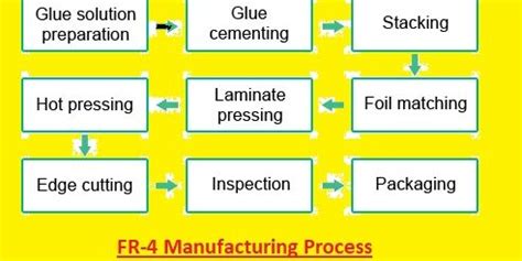
The FR4 PCB Manufacturing Process
The manufacturing process for FR4 PCBs involves a number of key steps:
1. Design and Data Preparation
The PCB design is created using EDA (electronic design automation) software. The design includes the copper tracking, solder pads, vias, and any other features. The Gerber files generated from the EDA package contain all the data required to manufacture the board.
2. Cutting FR4 Laminate Sheets
Sheets of FR4 copper clad laminate (CCL) are cut to the required size for the panel of PCBs to be produced. The sheets are usually 1.6mm thick but other thicknesses are used depending on the number of layers and the end application.
3. Drilling
The drill file from the Gerber data is used to drill all the holes in the panel. This includes holes for vias, through-hole component leads and mounting. CNC drilling machines are used which can drill multiple boards at the same time.
4. Copper Patterning
The copper tracks, pads and planes are formed on the FR4 substrate using a photolithography process:
- The panel is cleaned and a photoresist layer is applied
- The photoresist is exposed with UV light through a mask or by direct imaging
- The photoresist is developed, removing the exposed areas
- The exposed copper is etched away using an alkaline or acidic solution
- The remaining photoresist is stripped, leaving the copper pattern
This process is repeated for the copper pattern on the other side of the board for double-sided and multilayer boards.
5. Laminating
For multilayer boards, once the inner layers have been patterned, they are stacked with prepreg (pre-impregnated) sheets in between each layer. Prepreg is FR4 material that only partially cured. The stack is then laminated together under high temperature and pressure which cures the prepreg to form a solid board.
6. Solder Mask Application
A solder mask layer is applied to the outer layers of the board. This is a polymer coating that protects the copper from oxidation and prevents solder bridging between tracks. The solder mask is typically green but other colors are available. Photolithography is used to define the openings in the solder mask over pads and areas that need to be soldered.
7. Surface Finishes
To protect any exposed copper and to provide a solderable surface, a surface finish is applied to the PCB. The most common types are:
- HASL (Hot Air Solder Leveling) – the board is coated in molten solder and then hot air knives remove the excess leaving a thin layer of solder
- ENIG (Electroless Nickel Immersion Gold) – a thin layer of gold over a nickel barrier layer is plated onto the copper
- OSP (Organic Solderability Preservative) – an organic compound that provides a tarnish-resistant coating
The choice of surface finish depends on the components to be used and the soldering process.
8. Silkscreen
The silkscreen is the white text and symbols printed onto the solder mask. It is applied by screen printing an ink onto the board which is then cured. The silkscreen includes component identifiers, logos, and any other required markings.
9. Electrical Testing
To verify the PCB has been manufactured correctly, an electrical test is performed. A bed-of-nails test fixture or a flying probe is used to check for shorts, opens and correct continuity between nets. Any boards that fail are identified for rework or scrapped.
10. Final Cutting and Inspection
The individual boards are routed or snapped out of the panel. They undergo a final visual inspection and are packaged for shipping to the customer.

Advantages of Using FR4 for PCBs
There are a number of advantages to using FR4 as the base material for PCBs:
- Good electrical insulating properties with a high dielectric strength
- Mechanically strong and rigid while still being relatively lightweight
- Very good thermal resistance, with a Tg of 130°C to 180°C depending on grade
- Self-extinguishing and resistant to burning (UL 94 V-0 rated)
- Resistant to moisture absorption and chemicals
- Maintains performance over a wide temperature range (-55°C to +125°C)
- Can be made with high layer counts for complex designs
- Widely available from many manufacturers at a reasonable cost
These properties make FR4 suitable for use in a broad range of industries and applications including:
- Consumer electronics
- Telecommunications
- Aerospace and defence
- Automotive
- Industrial control
- Medical devices
FR4 has become the default material for the majority of PCB designs due to its excellent all-round performance and cost-effectiveness.

Limitations and Challenges of FR4 PCBs
While FR4 is an excellent material for most PCB applications, there are some limitations and challenges that need to be considered:
High Frequency Performance
The dielectric constant (Dk) of standard FR4 is relatively high at around 4.5. This limits its usability at very high frequencies above a few GHz. The high Dk results in significant signal loss in transmission lines. For high frequency RF and microwave designs, lower Dk materials such as Rogers 4003 or Teflon are typically used instead.
Thermal Management
FR4 has a relatively low thermal conductivity, which can make it difficult to dissipate heat from high power components. This can lead to issues with thermal management and reliability. To mitigate this, techniques such as using large copper pours, thermal vias, and heatsinks can be employed. For very high power applications, materials with higher thermal conductivity such as aluminum or copper core PCBs may be preferable.
Dimensional Stability
FR4 has a relatively high coefficient of thermal expansion (CTE) which can cause dimensional changes with temperature. This can be an issue for designs with fine pitch components or tight tolerances. The CTE of FR4 is also different in the X and Y axes due to the woven glass reinforcement. This anisotropic CTE can cause warpage of the board, particularly for thin laminates or asymmetric designs.
Moisture Absorption
Although FR4 has low moisture absorption compared to other materials, it can still absorb moisture from the environment over time. This can cause changes in the dielectric constant and affect electrical performance. It can also lead to delamination or blistering of the board during soldering processes. Proper storage and baking of the PCB prior to assembly can help to mitigate moisture related issues.
Despite these limitations, FR4 remains the most widely used material for PCBs due to its good all-round performance and cost-effectiveness. In most cases, the limitations can be overcome through proper design and manufacturing practices.

Frequently Asked Questions (FAQ)
1. What does FR4 stand for?
FR4 stands for “Flame Retardant 4”. The “4” denotes woven glass reinforced epoxy resin, and the “FR” indicates that it has flame retardant properties.
2. Is FR4 a good insulator?
Yes, FR4 has very good insulating properties. It has a dielectric strength of around 20 MV/m and a dielectric constant of 4.5 at 1 MHz. This makes it an excellent insulator for PCB substrates.
3. What is the difference between FR2 and FR4?
FR2 is a NEMA grade designation for phenolic paper laminate. It is not reinforced with glass fibers like FR4. FR2 is cheaper than FR4 but has lower mechanical and thermal performance. It is typically used for low-end consumer electronics. FR4 is superior to FR2 in almost all properties and is used for the majority of PCB applications.
4. Can FR4 be used for high frequency PCBs?
The high dielectric constant of standard FR4 (Dk = 4.5) limits its usefulness at high frequencies above a few GHz. The high Dk results in significant losses in transmission lines at high frequencies. For RF and microwave PCBs, lower Dk materials such as Rogers 4003 (Dk = 3.55) or Teflon (Dk = 2.1) are commonly used instead of FR4.
5. How many layers can an FR4 PCB have?
FR4 PCBs are commonly made with up to 16 layers, but can be manufactured with even higher layer counts. The maximum number of layers possible depends on the thickness of the laminate and the minimum via size that can be reliably manufactured. Boards with 30+ layers are possible but are very challenging to manufacture and are only used for the most complex designs. High layer count boards are used in applications such as supercomputers, telecommunications infrastructure, and high-end medical equipment.
Leave a Reply