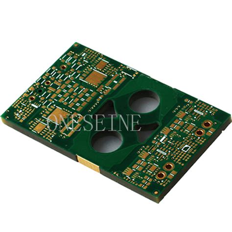
Introduction to Heavy Copper PCB
Heavy Copper PCBs, also known as thick copper PCBs or high current PCBs, are printed circuit boards that feature thicker copper traces than standard PCBs. These specialized boards are designed to handle higher currents and provide better thermal management, making them ideal for applications that require high power delivery or generate significant heat.
Key Characteristics of Heavy Copper PCBs
- Thicker copper traces (typically 3 oz or more)
- Improved current carrying capacity
- Enhanced thermal dissipation
- Increased mechanical strength and durability
- Suitable for high-power applications
Benefits of Using Heavy Copper PCBs
Increased Current Carrying Capacity
One of the primary advantages of heavy copper PCBs is their ability to handle higher currents compared to standard PCBs. The thicker copper traces allow for greater current flow without experiencing excessive voltage drops or overheating. This makes heavy copper PCBs well-suited for power electronics, motor drives, and other high-current applications.
| Copper Thickness | Current Carrying Capacity (per mm width) |
|---|---|
| 1 oz (35 µm) | 1.4 A |
| 2 oz (70 µm) | 2.8 A |
| 3 oz (105 µm) | 4.2 A |
| 4 oz (140 µm) | 5.6 A |
Improved Thermal Management
Heavy copper PCBs offer superior thermal management compared to standard PCBs. The thicker copper traces provide a larger surface area for heat dissipation, allowing the board to efficiently transfer heat away from components. This helps to prevent overheating and ensures stable operation, even in high-temperature environments.
Enhanced Mechanical Strength and Durability
The increased copper thickness in heavy copper PCBs also contributes to their mechanical strength and durability. These boards are less susceptible to damage from vibration, shock, and thermal stress. The thicker copper traces provide a more robust foundation for components, reducing the risk of trace cracking or delamination over time.

Applications of Heavy Copper PCBs
Power Electronics
Heavy copper PCBs are commonly used in power electronics applications, such as:
- Power supplies
- Inverters
- Motor drives
- Battery management systems
- Renewable energy systems
The high current carrying capacity and improved thermal management of heavy copper PCBs make them well-suited for handling the high power demands of these applications.
Automotive Electronics
In the automotive industry, heavy copper PCBs are used in various electronic systems, including:
- Engine control units (ECUs)
- Transmission control modules
- Electric power steering systems
- Electric vehicle charging systems
- Hybrid and electric vehicle battery management systems
The robust nature of heavy copper PCBs ensures reliable performance in the harsh operating conditions encountered in automotive applications.
Industrial Automation and Control
Heavy copper PCBs are also employed in industrial automation and control systems, such as:
- Programmable logic controllers (PLCs)
- Servo drives
- Industrial robots
- Motor control systems
- Power distribution systems
The improved current handling and thermal management capabilities of heavy copper PCBs enable these systems to operate efficiently and reliably in demanding industrial environments.

Designing Heavy Copper PCBs
Copper Thickness Selection
When designing a heavy copper PCB, the first step is to determine the appropriate copper thickness based on the current requirements of the application. The table below provides a general guideline for selecting copper thickness based on current density:
| Current Density (A/mm²) | Recommended Copper Thickness |
|---|---|
| 0.2 – 0.5 | 1 oz (35 µm) |
| 0.5 – 1.0 | 2 oz (70 µm) |
| 1.0 – 1.5 | 3 oz (105 µm) |
| 1.5 – 2.0 | 4 oz (140 µm) |
It is important to consider the specific requirements of your application and consult with your PCB manufacturer to determine the optimal copper thickness.
Thermal Management Considerations
When designing heavy copper PCBs, thermal management is a critical consideration. In addition to selecting the appropriate copper thickness, designers should also:
- Optimize component placement to minimize heat generation and improve heat dissipation
- Use thermal vias to transfer heat from components to the PCB’s copper layers
- Incorporate heat sinks or other cooling solutions when necessary
- Consider using thermal interface materials to improve heat transfer between components and the PCB
By addressing thermal management during the design process, designers can ensure that their heavy copper PCBs operate reliably and efficiently.
Manufacturing Considerations
Manufacturing heavy copper PCBs requires specialized processes and equipment due to the increased copper thickness. Some key considerations include:
- Longer etching times to achieve the desired trace thickness
- Increased drilling and plating times for through-holes and vias
- Potential for increased warpage due to the higher thermal mass of the thicker copper layers
- Higher material costs compared to standard PCBs
Designers should work closely with their PCB manufacturer to ensure that their heavy copper PCB designs are optimized for manufacturability and cost-effectiveness.

Conclusion
Heavy copper PCBs offer numerous benefits over standard PCBs, including increased current carrying capacity, improved thermal management, and enhanced mechanical strength and durability. These advantages make them ideal for applications in power electronics, automotive systems, and industrial automation and control.
When designing heavy copper PCBs, it is essential to consider factors such as copper thickness selection, thermal management, and manufacturing considerations. By addressing these aspects during the design process and working closely with a knowledgeable PCB manufacturer, designers can create robust and reliable heavy copper PCBs that meet the demands of their specific applications.
Frequently Asked Questions (FAQ)
1. What is the difference between heavy copper PCBs and standard PCBs?
Heavy copper PCBs feature thicker copper traces than standard PCBs, typically 3 oz (105 µm) or more. This increased copper thickness allows for higher current carrying capacity, improved thermal management, and enhanced mechanical strength and durability.
2. What are the main applications for heavy copper PCBs?
Heavy copper PCBs are commonly used in applications that require high power delivery or generate significant heat, such as power electronics, automotive systems, and industrial automation and control. Examples include power supplies, motor drives, engine control units, and programmable logic controllers.
3. How do I select the appropriate copper thickness for my heavy copper PCB?
The appropriate copper thickness for a heavy copper PCB depends on the current requirements of the application. A general guideline is to use 1 oz (35 µm) for current densities between 0.2 – 0.5 A/mm², 2 oz (70 µm) for 0.5 – 1.0 A/mm², 3 oz (105 µm) for 1.0 – 1.5 A/mm², and 4 oz (140 µm) for 1.5 – 2.0 A/mm². However, it is essential to consider the specific requirements of your application and consult with your PCB manufacturer for optimal copper thickness selection.
4. What are the key thermal management considerations when designing heavy copper PCBs?
When designing heavy copper PCBs, key thermal management considerations include optimizing component placement to minimize heat generation and improve heat dissipation, using thermal vias to transfer heat from components to the PCB’s copper layers, incorporating heat sinks or other cooling solutions when necessary, and considering the use of thermal interface materials to improve heat transfer between components and the PCB.
5. Are there any manufacturing challenges associated with heavy copper PCBs?
Yes, manufacturing heavy copper PCBs requires specialized processes and equipment due to the increased copper thickness. Some challenges include longer etching times to achieve the desired trace thickness, increased drilling and plating times for through-holes and vias, potential for increased warpage due to the higher thermal mass of the thicker copper layers, and higher material costs compared to standard PCBs. Designers should work closely with their PCB manufacturer to ensure that their heavy copper PCB designs are optimized for manufacturability and cost-effectiveness.
Leave a Reply