Introduction to Copper PCBs
Printed Circuit Boards (PCBs) are essential components in modern electronics, providing a platform for interconnecting electronic components and enabling the functioning of complex circuits. Among the various types of PCBs, thick copper PCBs have gained significant attention due to their unique characteristics and advantages in specific applications. In this article, we will delve into the world of thick copper PCBs, exploring their features, manufacturing process, applications, and more.
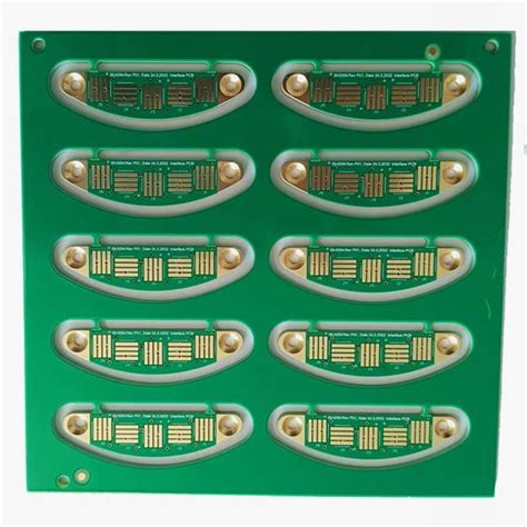
What are Copper PCBs?
Copper PCBs are printed circuit boards that utilize copper as the primary conductive material for the traces and pads. Copper is chosen for its excellent electrical conductivity, thermal conductivity, and durability. The thickness of the copper layer in a PCB can vary depending on the specific requirements of the application. Thick copper PCBs, as the name suggests, feature a thicker copper layer compared to standard PCBs.
Advantages of Thick Copper PCBs
Thick copper PCBs offer several advantages over standard PCBs:
-
Enhanced Current Carrying Capacity: The increased thickness of the copper layer allows thick copper PCBs to handle higher currents without overheating or experiencing voltage drops.
-
Improved Thermal Management: The thicker copper layer provides better thermal conductivity, allowing for more efficient heat dissipation from components mounted on the PCB.
-
Increased Mechanical Strength: Thick copper PCBs exhibit higher mechanical strength and durability, making them suitable for applications that require robust and reliable performance.
-
Reduced Electrical Resistance: The thicker copper layer results in lower electrical resistance, minimizing power losses and improving overall circuit efficiency.
Manufacturing Process of Thick Copper PCBs
The manufacturing process of thick copper PCBs involves several key steps:
1. Substrate Preparation
The process begins with the preparation of the PCB substrate, typically made of FR-4 or other suitable materials. The substrate is cleaned and treated to ensure proper adhesion of the copper layer.
2. Copper Deposition
Thick copper is deposited onto the substrate using various methods, such as electroplating or foil lamination. The desired thickness of the copper layer is achieved through precise control of the deposition process.
3. Patterning and Etching
The copper layer is then patterned using photolithography techniques. A photoresist layer is applied, exposed to UV light through a patterned mask, and developed to create the desired circuit pattern. The exposed copper areas are etched away, leaving behind the required traces and pads.
4. Drilling and Plating
Holes are drilled through the PCB to accommodate through-hole components and vias. The holes are then plated with copper to establish electrical connections between layers.
5. Solder Mask and Silkscreen
A solder mask layer is applied to the PCB to protect the copper traces and prevent short circuits. Silkscreen printing is used to add component labels, logos, and other markings on the PCB surface.
6. Surface Finishing
The exposed copper areas, such as pads and contacts, are coated with a surface finish to prevent oxidation and enhance solderability. Common surface finishes include HASL (Hot Air Solder Leveling), ENIG (Electroless Nickel Immersion Gold), and OSP (Organic Solderability Preservative).

Applications of Thick Copper PCBs
Thick copper PCBs find applications in various industries and domains where high current handling, thermal management, and mechanical strength are critical. Some notable applications include:
1. Power Electronics
Thick copper PCBs are extensively used in power electronic systems, such as power converters, inverters, and motor drives. The high current carrying capacity and efficient heat dissipation provided by thick copper traces make them ideal for handling high power densities.
2. Automotive Electronics
In the automotive industry, thick copper PCBs are employed in various electronic systems, including engine control units (ECUs), power distribution modules, and battery management systems. The increased mechanical strength and thermal stability of thick copper PCBs ensure reliable performance in the harsh automotive environment.
3. Industrial Control Systems
Industrial control systems often require PCBs that can withstand high currents and extreme operating conditions. Thick copper PCBs are well-suited for applications such as motor controls, power supplies, and industrial automation equipment.
4. LED Lighting
LED lighting applications benefit from thick copper PCBs due to their ability to efficiently dissipate heat generated by high-power LEDs. The improved thermal management helps maintain optimal LED performance and longevity.
5. Aerospace and Defense
Thick copper PCBs are used in aerospace and defense applications where reliability and durability are paramount. They are found in avionics systems, radar equipment, and military communication devices.

Design Considerations for Thick Copper PCBs
When designing thick copper PCBs, several factors need to be taken into account:
1. Copper Thickness
The thickness of the copper layer should be determined based on the current carrying requirements and thermal management needs of the application. Common thick copper thicknesses range from 3 oz/ft² to 10 oz/ft² or more.
2. Trace Width and Spacing
The width and spacing of copper traces should be designed to accommodate the desired current flow while maintaining appropriate clearances to prevent short circuits and ensure manufacturability.
3. Thermal Management
Proper thermal management techniques should be employed to dissipate heat effectively from components mounted on the PCB. This may involve the use of thermal vias, heat sinks, or other cooling methods.
4. Mechanical Considerations
The increased thickness of the copper layer can impact the mechanical properties of the PCB. Factors such as flexibility, rigidity, and drilling capabilities should be considered during the design phase.
5. Cost and Manufacturing Feasibility
Thick copper PCBs typically have higher manufacturing costs compared to standard PCBs due to the additional copper material and processing steps involved. The design should be optimized to balance cost and performance while ensuring manufacturing feasibility.

Copper Thickness Comparison
The following table provides a comparison of common copper thicknesses used in PCBs:
| Copper Thickness (oz/ft²) | Thickness (mm) | Typical Applications |
|---|---|---|
| 0.5 | 0.017 | Low-power, high-density designs |
| 1 | 0.035 | General-purpose PCBs |
| 2 | 0.070 | Medium-power and mixed-signal designs |
| 3 | 0.105 | Power electronics and automotive |
| 4 | 0.140 | High-power and industrial control systems |
| 6 | 0.210 | Extreme high-power applications |
| 10 | 0.350 | Specialized high-current applications |
Frequently Asked Questions (FAQ)
1. What is the difference between thick copper PCBs and standard PCBs?
Thick copper PCBs have a thicker copper layer compared to standard PCBs. The increased copper thickness provides higher current carrying capacity, improved thermal management, and increased mechanical strength.
2. What are the common applications of thick copper PCBs?
Thick copper PCBs are commonly used in power electronics, automotive electronics, industrial control systems, LED lighting, aerospace, and defense applications where high current handling and thermal management are critical.
3. How thick is the copper layer in thick copper PCBs?
The thickness of the copper layer in thick copper PCBs typically ranges from 3 oz/ft² to 10 oz/ft² or more, depending on the specific requirements of the application.
4. What are the advantages of using thick copper PCBs?
The advantages of using thick copper PCBs include enhanced current carrying capacity, improved thermal management, increased mechanical strength, and reduced electrical resistance.
5. Are thick copper PCBs more expensive than standard PCBs?
Yes, thick copper PCBs generally have higher manufacturing costs compared to standard PCBs due to the additional copper material and processing steps involved. However, the benefits they offer in terms of performance and reliability often justify the increased cost in specific applications.
Conclusion
Thick copper PCBs play a vital role in various industries and applications where high current handling, efficient thermal management, and mechanical robustness are essential. By utilizing a thicker copper layer, these PCBs offer enhanced electrical and thermal performance, making them suitable for power electronics, automotive systems, industrial controls, and more.
When designing thick copper PCBs, careful consideration must be given to factors such as copper thickness, trace width and spacing, thermal management, and mechanical properties. Balancing cost and performance while ensuring manufacturing feasibility is also crucial.
As technology advances and the demand for high-performance electronics grows, thick copper PCBs will continue to be an important solution for addressing the challenges of power density, heat dissipation, and reliability. By understanding the characteristics, manufacturing process, and applications of thick copper PCBs, designers and engineers can leverage their benefits to create innovative and robust electronic systems.
Leave a Reply