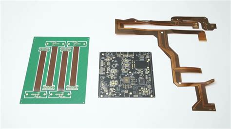
What is a Flexible PCB?
A flexible printed circuit board (PCB), also known as a flex circuit, is a type of PCB that consists of a thin insulating polymer film with conductive copper traces. Unlike traditional rigid PCBs, flexible PCBs can bend, twist, and fold to fit into tight spaces or conform to unique shapes. This versatility makes them ideal for applications requiring compact packaging, dynamic flexing, or high-density interconnections.
Key Features of Flexible PCBs
- Thin and lightweight
- High flexibility and durability
- Excellent thermal stability
- Resistance to vibration and shock
- Ability to accommodate complex geometries
Applications of Flexible PCBs
Flexible PCBs find extensive use in various industries due to their unique properties and advantages over rigid PCBs. Some common applications include:
- Consumer electronics (smartphones, wearables, cameras)
- Medical devices (implantable devices, diagnostic equipment)
- Automotive electronics (dashboard displays, sensors)
- Aerospace and defense (avionics, satellites, missiles)
- Industrial automation (robotics, machine vision systems)

Types of Flexible PCBs
There are three main types of flexible PCBs based on their construction and layer count:
- Single-sided flex PCBs
- Consist of a single conductive layer on a flexible substrate
-
Suitable for simple, low-density designs
-
Double-sided flex PCBs
- Have two conductive layers with vias connecting them
-
Offer higher circuit density and design flexibility
-
Multi-layer flex PCBs
- Contain three or more conductive layers separated by insulating layers
- Provide the highest circuit density and complexity

Flexible PCB Manufacturing Process
The manufacturing process for flexible PCBs involves several key steps, as outlined below:
Step 1: Design and Layout
- Create a schematic diagram and PCB layout using CAD software
- Consider flex-specific design rules (bend radius, trace width, via size)
- Perform design rule checks (DRC) and generate manufacturing files
Step 2: Material Selection
- Choose appropriate flexible substrate (e.g., polyimide, PET)
- Select copper foil thickness and grade (e.g., RA, ED)
- Consider coverlay or soldermask materials for protection
Step 3: Lamination
- Laminate copper foil to the flexible substrate using heat and pressure
- For multi-layer boards, laminate multiple layers together with adhesive
Step 4: Drilling and Routing
- Drill through-holes and vias using laser or mechanical drilling
- Route the board outline and any internal cutouts
Step 5: Patterning
- Apply and expose photoresist to define the circuit pattern
- Develop the photoresist to reveal the desired copper traces
- Etch away unwanted copper using chemical etching
Step 6: Surface Finishing
- Apply surface finish to exposed copper (e.g., ENIG, OSP, HASL)
- Protect the copper from oxidation and improve solderability
Step 7: Solder Mask Application
- Apply and expose soldermask to protect the circuitry
- Develop and cure the soldermask
Step 8: Silkscreen Printing
- Print component designators, logos, and other markings using silkscreen
Step 9: Coverlay Lamination (optional)
- Laminate a coverlay film over the circuitry for additional protection
- Openings in the coverlay allow access to pads and connection points
Step 10: Cutting and Singulation
- Cut the panel into individual flexible PCBs
- Use laser cutting, die-cutting, or routing for precise singulation
Step 11: Electrical Testing
- Perform electrical continuity and insulation resistance tests
- Verify the functionality of the flexible PCBs
Step 12: Final Inspection and Packaging
- Visually inspect the boards for defects and cosmetic issues
- Package the flexible PCBs for shipping and delivery

Comparing Flexible PCB Manufacturing to Rigid PCB Manufacturing
While the overall manufacturing process for flexible PCBs is similar to that of rigid PCBs, there are some key differences to consider:
| Aspect | Flexible PCBs | Rigid PCBs |
|---|---|---|
| Substrate Material | Thin, flexible polymer films (e.g., polyimide, PET) | Rigid, fiber-reinforced epoxy laminate (e.g., FR-4) |
| Thickness | Typically thinner (0.1–0.3 mm) | Thicker (0.4–3.2 mm) |
| Lamination Process | Adhesive bonding or thermal bonding | Pressure and heat lamination |
| Drilling | Laser drilling more common for small, precise holes | Mechanical drilling more common |
| Coverlay | Optional, provides additional protection | Not applicable |
| Cutting and Singulation | Laser cutting, die-cutting, or routing | Routing or punching |
Advantages of Flexible PCBs over Rigid PCBs
- Reduced weight and size
- Improved reliability in dynamic and high-stress environments
- Enhanced design freedom and form factor flexibility
- Simplified assembly and reduced interconnections
- Potential for cost savings in certain applications
Challenges in Flexible PCB Manufacturing
Despite their numerous benefits, flexible PCBs present some unique challenges during manufacturing:
- Handling and processing thin, delicate materials
- Maintaining proper alignment and registration during lamination
- Controlling dimensional stability during thermal processes
- Ensuring reliable plated through-holes and vias
- Preventing damage during flexing and bending operations
Future Trends in Flexible PCB Manufacturing
As technology advances and demand for compact, high-performance electronics grows, flexible PCB manufacturing is likely to evolve in the following ways:
- Increased adoption of high-density interconnect (HDI) designs
- Development of advanced materials with improved thermal and mechanical properties
- Greater integration of embedded components and active devices
- Expansion of 3D printing technologies for rapid prototyping and low-volume production
- Growing use of flexible hybrid electronics (FHE) for wearable and IoT applications
FAQ
1. What is the typical turnaround time for flexible PCB manufacturing?
The turnaround time for flexible PCB manufacturing can vary depending on the complexity of the design, the materials used, and the manufacturer’s capacity. On average, lead times range from 2-4 weeks for standard designs and up to 6-8 weeks for more complex or customized orders.
2. How do I choose the right flexible substrate material for my application?
When selecting a flexible substrate material, consider factors such as the required flexibility, temperature range, dielectric properties, and cost. Polyimide (PI) and polyethylene terephthalate (PET) are two common choices, with PI offering better thermal stability and durability, while PET is more cost-effective for less demanding applications.
3. Can flexible PCBs be used in high-temperature environments?
Yes, flexible PCBs can be designed to withstand high-temperature environments. Polyimide substrates, in particular, have excellent thermal stability and can maintain their properties at temperatures up to 300°C. However, it’s essential to consider the temperature ratings of all materials used in the PCB, including the conductors, adhesives, and coatings.
4. What is the minimum bend radius for a flexible PCB?
The minimum bend radius for a flexible PCB depends on several factors, including the substrate material, copper thickness, and the number of layers. As a general rule, the minimum bend radius should be at least 6 times the total thickness of the PCB. For example, a 0.2 mm thick PCB should have a minimum bend radius of 1.2 mm. Consult with your manufacturer for specific recommendations based on your design.
5. How can I ensure the reliability of my flexible PCB design?
To ensure the reliability of your flexible PCB design, follow these best practices:
- Use appropriate materials and thicknesses for your application
- Follow the manufacturer’s design guidelines for trace width, spacing, and bend radius
- Incorporate strain relief features, such as stiffeners or support structures, in high-stress areas
- Perform thorough testing and validation, including mechanical and environmental stress tests
- Work closely with your manufacturer to optimize your design for manufacturability and reliability
By understanding the unique characteristics and manufacturing processes of flexible PCBs, designers can create reliable, high-performance products that leverage the benefits of this versatile technology.
Leave a Reply