Introduction to PCB Capacitance
Printed Circuit Boards (PCBs) are essential components in modern electronics, providing a platform for interconnecting various electronic components. One crucial aspect of PCB Design is understanding and managing the capacitance between traces and planes. This article delves into the concept of PCB trace to plane capacitance, its importance, and the formula used to calculate it.
What is PCB Capacitance?
PCB capacitance refers to the electrical property of a PCB that allows it to store electric charge. In a PCB, capacitance exists between conductive layers, such as traces and planes. When a voltage is applied across these layers, an electric field is generated, resulting in the storage of electric charge. This stored charge can influence the behavior of signals propagating through the PCB.
Importance of PCB Capacitance
Understanding and managing PCB capacitance is crucial for several reasons:
-
Signal Integrity: Capacitance between traces and planes can impact the quality of signals transmitted through the PCB. Excessive capacitance can lead to signal distortion, crosstalk, and increased propagation delay.
-
Impedance Matching: Proper management of PCB capacitance is essential for achieving impedance matching, which ensures optimal signal transmission and minimizes reflections.
-
Power Distribution: Capacitance plays a role in the power distribution network of a PCB. Decoupling capacitors, which rely on the capacitance between planes, help stabilize the power supply and reduce noise.
-
Electromagnetic Compatibility (EMC): PCB capacitance can affect the electromagnetic compatibility of a device. Unintended capacitance can contribute to electromagnetic interference (EMI) and impact the overall EMC performance.
Factors Affecting PCB Trace to Plane Capacitance
Several factors influence the capacitance between a PCB trace and a plane:
Dielectric Material
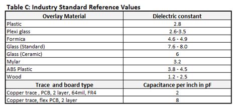
The dielectric material used in the PCB plays a significant role in determining the capacitance. The dielectric constant (εr) of the material directly affects the capacitance value. Common dielectric materials used in PCBs include FR-4, Rogers, and polyimide.
Trace Geometry
The geometry of the PCB trace, including its width, thickness, and length, impacts the capacitance. Wider and thicker traces generally have higher capacitance compared to narrower and thinner traces.
Plane Separation
The distance between the trace and the plane, known as the plane separation, influences the capacitance. A smaller plane separation results in higher capacitance, while a larger separation reduces the capacitance.
Frequency
The operating frequency of the signals propagating through the PCB affects the effective capacitance. At higher frequencies, the capacitive reactance decreases, making the capacitance more significant.

PCB Trace to Plane Capacitance Formula
The capacitance between a PCB trace and a plane can be calculated using the following formula:
C = (ε0 × εr × A) / d
Where:
– C is the capacitance in farads (F)
– ε0 is the permittivity of free space (8.85 × 10^-12 F/m)
– εr is the relative permittivity (dielectric constant) of the dielectric material
– A is the area of overlap between the trace and the plane in square meters (m^2)
– d is the distance between the trace and the plane in meters (m)
To use this formula effectively, follow these steps:
-
Determine the dielectric constant (εr) of the PCB material. Consult the material specifications or manufacturer’s datasheet.
-
Calculate the area of overlap (A) between the trace and the plane. This can be done by multiplying the trace width by its length over the plane.
-
Measure the distance (d) between the trace and the plane. This is typically the thickness of the dielectric layer separating them.
-
Substitute the values into the formula and perform the calculation to obtain the capacitance value.
Here’s an example calculation:
Let’s say we have a PCB with the following parameters:
– Dielectric material: FR-4 (εr = 4.5)
– Trace width: 0.2 mm
– Trace length over the plane: 50 mm
– Distance between trace and plane: 0.1 mm
Step 1: Dielectric constant (εr) = 4.5
Step 2: Area of overlap (A) = 0.2 mm × 50 mm = 10 mm^2 = 10 × 10^-6 m^2
Step 3: Distance between trace and plane (d) = 0.1 mm = 0.1 × 10^-3 m
Step 4: Capacitance calculation:
C = (8.85 × 10^-12 F/m × 4.5 × 10 × 10^-6 m^2) / (0.1 × 10^-3 m)
C = 3.98 × 10^-13 F = 0.398 pF
So, the capacitance between the trace and the plane in this example is approximately 0.398 picofarads (pF).

Managing PCB Trace to Plane Capacitance
Proper management of PCB trace to plane capacitance is essential for optimal circuit performance. Here are some strategies to control and optimize capacitance:
Dielectric Material Selection
Choose a dielectric material with a suitable dielectric constant based on the desired capacitance and other design requirements. Materials with lower dielectric constants, such as Rogers or polyimide, can help reduce capacitance compared to FR-4.
Trace Geometry Optimization
Optimize the trace geometry to achieve the desired capacitance. Narrower and thinner traces generally have lower capacitance. However, consider the trade-offs with signal integrity and manufacturability.
Plane Separation Adjustment
Increase the distance between the trace and the plane to reduce capacitance. This can be achieved by using thicker dielectric layers or strategically placing traces on different layers.
Ground Plane Usage
Utilize ground planes effectively to provide a low-impedance return path for signals. Proper grounding helps minimize the impact of unwanted capacitance on signal integrity.
Simulation and Modeling
Employ PCB Simulation and modeling tools to analyze and optimize capacitance. These tools can help predict capacitance values, identify potential issues, and guide design decisions.

Frequently Asked Questions (FAQ)
-
What is the main factor that determines PCB trace to plane capacitance?
The main factors that determine PCB trace to plane capacitance are the dielectric constant of the PCB material, the area of overlap between the trace and the plane, and the distance between the trace and the plane. -
How does increasing the dielectric constant affect PCB capacitance?
Increasing the dielectric constant of the PCB material leads to higher capacitance between traces and planes. A higher dielectric constant means the material has a greater ability to store electric charge. -
What is the impact of high PCB capacitance on signal integrity?
High PCB capacitance can negatively impact signal integrity. Excessive capacitance can cause signal distortion, increase propagation delay, and contribute to crosstalk between adjacent traces. -
How can PCB trace to plane capacitance be reduced?
PCB trace to plane capacitance can be reduced by selecting a dielectric material with a lower dielectric constant, optimizing trace geometry (narrower and thinner traces), increasing the distance between the trace and the plane, and utilizing ground planes effectively. -
Why is it important to manage PCB capacitance in high-speed designs?
Managing PCB capacitance is crucial in high-speed designs because capacitance becomes more significant at higher frequencies. Unmanaged capacitance can lead to signal integrity issues, such as reflections, crosstalk, and increased propagation delay, which can compromise the performance and reliability of high-speed circuits.
Conclusion
Understanding and managing PCB trace to plane capacitance is crucial for designing reliable and high-performance electronic circuits. The capacitance formula presented in this article provides a foundation for calculating the capacitance between traces and planes. By considering factors such as dielectric material, trace geometry, plane separation, and frequency, designers can optimize PCB Layouts to achieve desired capacitance values and mitigate potential signal integrity issues.
Effective management of PCB capacitance involves careful selection of dielectric materials, optimization of trace geometry, adjustment of plane separation, proper usage of ground planes, and utilization of simulation and modeling tools. By following best practices and understanding the impact of capacitance on signal integrity, designers can create PCBs that meet the demanding requirements of modern electronics.
As technology advances and signal speeds continue to increase, the importance of managing PCB capacitance becomes even more critical. By staying informed about the latest techniques and tools for capacitance control, PCB designers can ensure the success and reliability of their designs in today’s rapidly evolving electronic landscape.
Leave a Reply