Introduction to Castellated PCB
Castellated PCB, also known as castellated holes or castellations, is a type of printed circuit board (PCB) design feature that provides an alternative method for connecting and mounting components to the board. This technique involves creating semi-circular holes or slots along the edges of the PCB, which allows for the easy attachment of modules or other PCBs without the need for additional connectors or wires.
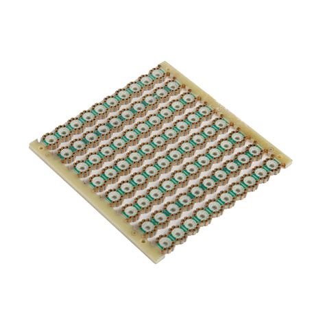
What are Castellated Holes?
Castellated holes are semi-circular holes drilled or routed into the edge of a PCB. These holes are typically plated with a conductive material, such as copper, to establish electrical connections between the PCB and the attached module. The term “castellated” derives from the resemblance of these holes to the battlements of a castle wall.
Advantages of Castellated PCB Design
Castellated PCB design offers several advantages over traditional connection methods:
- Space-saving: Castellated holes eliminate the need for additional connectors, which can save valuable space on the PCB and reduce overall board size.
- Cost-effective: By eliminating the need for connectors, castellated PCB design can reduce material and assembly costs.
- Simplified assembly: Castellated holes allow for easy attachment of modules or other PCBs, simplifying the assembly process and reducing the risk of connection errors.
- Improved signal integrity: Direct connections through castellated holes can minimize signal loss and improve overall signal integrity compared to using connectors.
Plated Half Hole PCB Castellated Hole
Plated half hole PCB castellated hole is a specific type of castellated hole design where the holes are not fully drilled through the PCB, but instead are drilled halfway through the board thickness. This design offers additional benefits and is particularly useful in certain applications.
How Plated Half Hole Castellations Work
In a plated half hole PCB castellated hole design, the holes are drilled or routed to a depth of approximately half the thickness of the PCB. The holes are then plated with a conductive material, typically copper, to create electrical connections. The exposed copper on the surface of the PCB allows for the attachment of modules or other PCBs using soldering techniques.
Benefits of Plated Half Hole Castellations
Plated half hole castellations offer several benefits over full-depth castellated holes:
- Increased mechanical strength: By leaving a portion of the PCB material beneath the castellated hole, the overall mechanical strength of the board is improved, reducing the risk of damage during handling or assembly.
- Enhanced solderability: The exposed copper on the surface of the PCB provides a larger surface area for soldering, ensuring a stronger and more reliable connection between the PCB and the attached module.
- Improved alignment: Plated half hole castellations can help guide and align the attached module during the soldering process, reducing the risk of misalignment or connection errors.
Applications of Plated Half Hole Castellated PCBs
Plated half hole castellated PCBs find applications in various industries and products, such as:
- Wearable devices: The space-saving and lightweight nature of castellated PCBs make them ideal for use in wearable devices, such as smartwatches or fitness trackers.
- IoT modules: Castellated PCBs are commonly used in Internet of Things (IoT) modules, where multiple sensors or communication modules need to be connected to a main board.
- Automotive electronics: The enhanced mechanical strength and reliability of plated half hole castellations make them suitable for use in automotive electronic systems, which are subject to vibrations and harsh environmental conditions.
- Aerospace and defense: Castellated PCBs are used in aerospace and defense applications, where high reliability and space optimization are critical factors.

Designing Plated Half Hole PCB Castellated Holes
When designing plated half hole PCB castellated holes, several factors must be considered to ensure optimal performance and manufacturability.
Hole Size and Spacing
The size and spacing of castellated holes are critical design considerations. The hole diameter should be large enough to accommodate the plating process and provide sufficient surface area for soldering. However, the holes should not be too large, as this can weaken the mechanical strength of the PCB.
The spacing between castellated holes is equally important, as it affects the overall size of the PCB and the routing of traces. The spacing should be sufficient to maintain the structural integrity of the board while allowing for the necessary electrical connections.
| Parameter | Recommended Value |
|---|---|
| Hole Diameter | 0.8 mm – 1.2 mm |
| Hole Spacing (Edge-to-Edge) | 1.0 mm – 2.0 mm |
| Copper Plating Thickness | 25 μm – 35 μm |
PCB Thickness and Material
The thickness of the PCB and the choice of material are also important considerations when designing plated half hole castellations. The PCB thickness should be sufficient to accommodate the depth of the castellated holes while maintaining the necessary mechanical strength. Common PCB thicknesses for castellated designs range from 0.8 mm to 1.6 mm.
The choice of PCB material depends on the specific application and requirements, such as operating temperature, dielectric constant, and cost. Common materials used for castellated PCBs include FR-4, Rogers, and polyimide.
Plating and Surface Finish
The plating and surface finish of castellated holes are critical for ensuring reliable electrical connections and solderability. Copper plating is the most common choice for castellated holes, with a typical thickness of 25 μm to 35 μm.
The surface finish of the PCB also affects the solderability and durability of the castellated connections. Common surface finishes for castellated PCBs include:
- HASL (Hot Air Solder Leveling): A cost-effective and widely used surface finish that provides good solderability and durability.
- ENIG (Electroless Nickel Immersion Gold): Offers excellent solderability, corrosion resistance, and a flat surface for improved connection reliability.
- OSP (Organic Solderability Preservative): A cost-effective and environmentally friendly surface finish that provides good solderability, although with a limited shelf life.

Manufacturing Plated Half Hole PCB Castellated Holes
The manufacturing process for plated half hole PCB castellated holes involves several steps to ensure the desired quality and performance.
Drilling or Routing
The first step in manufacturing castellated holes is drilling or routing the holes into the PCB. This process is typically performed using computer numerical control (CNC) machines, which ensure precise hole placement and depth control. The choice between drilling and routing depends on the specific design requirements and the available manufacturing equipment.
Plating
After drilling or routing, the castellated holes are plated with a conductive material, typically copper. The plating process involves several sub-steps:
- Desmear: Removes any debris or resin smear from the drilled holes to ensure proper plating adhesion.
- Electroless copper: Deposits a thin layer of copper onto the hole walls using a chemical process, providing a conductive base for subsequent plating.
- Electrolytic copper: Builds up the copper plating thickness to the desired level using an electric current in a copper sulfate solution.
Surface Finishing
Once the castellated holes are plated, the PCB undergoes the chosen surface finishing process (HASL, ENIG, or OSP) to protect the copper and enhance solderability. The surface finish is applied to the entire PCB, including the castellated holes and exposed copper surfaces.
Inspection and Quality Control
Throughout the manufacturing process, various inspection and quality control measures are implemented to ensure the plated half hole castellations meet the required specifications. These measures may include:
- Visual inspection: Checking for any visible defects, such as holes misalignment, incomplete plating, or surface finish irregularities.
- Electrical testing: Verifying the continuity and resistance of the castellated connections to ensure proper electrical performance.
- Microsectioning: Analyzing cross-sections of the castellated holes to assess plating thickness, hole geometry, and any internal defects.
By adhering to strict manufacturing processes and quality control measures, manufacturers can produce high-quality plated half hole PCB castellated holes that meet the demanding requirements of various applications.

Designing with Plated Half Hole Castellated PCBs
When designing a product that incorporates plated half hole castellated PCBs, several considerations should be taken into account to ensure optimal performance and reliability.
Module Compatibility
Ensure that the modules or other PCBs that will be attached to the castellated PCB are compatible with the chosen castellated hole design. Consider factors such as the module’s pad size, spacing, and layout to ensure proper alignment and connection.
Soldering Process
The soldering process is critical for establishing reliable connections between the castellated PCB and the attached modules. Consider the following factors when designing the soldering process:
- Solder paste: Select a solder paste with the appropriate alloy composition, particle size, and flux activity for the specific application and surface finish.
- Stencil design: Design the solder paste stencil to ensure the proper amount of solder is deposited on the castellated holes and pads.
- Reflow profile: Develop a suitable reflow profile that considers the thermal requirements of the PCB material, components, and solder paste to achieve optimal solder joint formation.
Mechanical Considerations
When designing a product with plated half hole castellated PCBs, consider the mechanical aspects of the design to ensure the overall stability and reliability of the assembly. This includes:
- Mounting: Determine the appropriate mounting method for the castellated PCB, such as using screws, standoffs, or adhesives, to provide mechanical support and prevent excessive stress on the solder joints.
- Strain relief: Incorporate strain relief mechanisms, such as using flexible connections or providing adequate slack in cables, to minimize mechanical stress on the castellated connections during handling or operation.
- Vibration and shock: Assess the expected levels of vibration and shock the product will be subjected to and design the castellated PCB and its connections accordingly, using techniques such as underfill or conformal coating for added protection.
By carefully considering these design aspects and working closely with the PCB manufacturer and assembly partner, designers can create products that leverage the benefits of plated half hole castellated PCBs while ensuring optimal performance and reliability.
Troubleshooting and Common Issues
When working with plated half hole castellated PCBs, several common issues may arise during the manufacturing, assembly, or operation stages. Being aware of these issues and understanding troubleshooting techniques can help minimize their impact and ensure the success of the project.
Manufacturing Defects
Manufacturing defects can occur during the PCB fabrication process, affecting the quality and reliability of the plated half hole castellations. Common manufacturing defects include:
- Incomplete plating: If the plating process is not properly controlled, the castellated holes may have incomplete or uneven plating, leading to poor electrical connections or reduced mechanical strength.
- Hole misalignment: Misaligned castellated holes can cause difficulties in attaching modules or other PCBs, resulting in poor connections or mechanical stress on the solder joints.
- Surface finish defects: Issues with the surface finish, such as uneven coverage, contamination, or poor adhesion, can affect the solderability and durability of the castellated connections.
To minimize the occurrence of manufacturing defects, work with reputable PCB manufacturers who have experience in producing castellated PCBs and implement strict quality control measures throughout the fabrication process.
Assembly Issues
During the assembly process, various issues can arise that affect the quality and reliability of the castellated connections. Common assembly issues include:
- Solder bridging: Excessive solder paste or improper reflow can lead to solder bridging between adjacent castellated holes, causing short circuits or signal integrity issues.
- Poor solder joint formation: Insufficient solder, incorrect reflow profile, or contamination can result in weak or incomplete solder joints, compromising the electrical and mechanical integrity of the connections.
- Misalignment: If the attached modules or PCBs are not properly aligned with the castellated holes, it can lead to mechanical stress, poor connections, or even damage to the components.
To avoid assembly issues, ensure that the solder paste stencil design, reflow profile, and alignment fixtures are optimized for the specific castellated PCB design. Implement inspection and testing procedures to catch any issues early in the assembly process.
Operational Failures
Even if the castellated PCB is manufactured and assembled correctly, operational failures can still occur due to various factors, such as:
- Mechanical stress: Excessive mechanical stress, caused by vibration, shock, or improper handling, can lead to solder joint cracking or failure over time.
- Thermal cycling: Repeated exposure to temperature fluctuations can cause thermal expansion and contraction, putting stress on the castellated connections and potentially leading to solder joint fatigue or failure.
- Environmental factors: Exposure to moisture, corrosive agents, or other harsh environmental conditions can degrade the castellated connections over time, affecting their electrical and mechanical performance.
To minimize the risk of operational failures, consider the expected operating conditions during the design phase and incorporate appropriate protection measures, such as underfill, conformal coating, or ruggedized packaging. Regularly inspect and test the castellated connections to catch any potential issues before they lead to complete failure.
By being aware of these common issues and implementing appropriate design, manufacturing, assembly, and testing strategies, designers and manufacturers can effectively troubleshoot and mitigate problems associated with plated half hole castellated PCBs, ensuring the long-term reliability and performance of the end product.
Frequently Asked Questions (FAQ)
-
Q: What is the difference between plated half hole and full-depth castellated holes?
A: Plated half hole castellations are drilled to a depth of approximately half the PCB thickness, while full-depth castellations go through the entire board. Half hole castellations offer increased mechanical strength and improved solderability compared to full-depth castellations. -
Q: Can plated half hole castellated PCBs be used for high-frequency applications?
A: Yes, plated half hole castellated PCBs can be used for high-frequency applications. However, careful design considerations must be taken to ensure signal integrity, such as proper impedance matching, ground plane design, and minimizing the length of the castellated connections. -
Q: What is the minimum hole size for plated half hole castellations?
A: The minimum hole size for plated half hole castellations depends on the PCB manufacturer’s capabilities and the specific design requirements. Typically, hole diameters range from 0.8 mm to 1.2 mm, but smaller sizes may be possible with advanced manufacturing techniques. -
Q: How does the choice of surface finish affect the performance of plated half hole castellations?
A: The surface finish plays a crucial role in the solderability, durability, and corrosion resistance of plated half hole castellations. ENIG (Electroless Nickel Immersion Gold) provides excellent solderability and flat surface, while HASL (Hot Air Solder Leveling) offers a cost-effective and durable option. The choice of surface finish depends on the specific application requirements and budget. -
Q: Can plated half hole castellated PCBs be reworked if a module needs to be replaced?
A: Yes, plated half hole castellated PCBs can be reworked, but it requires careful handling and the appropriate tools and techniques. The rework process typically involves removing the old module, cleaning the castellated holes, and soldering a new module in place. However, repeated rework can degrade the quality of the castellated connections, so it should be minimized whenever possible.
Conclusion
Plated half hole PCB castellated holes offer a versatile and reliable solution for connecting modules or other PCBs to a main board, providing numerous benefits such as space savings, cost reduction, and improved signal integrity. By understanding the design considerations, manufacturing processes, and common issues associated with castellated PCBs, designers and manufacturers can effectively leverage this technology to create high-performance, reliable products for a wide range of applications.
As the electronics industry continues to evolve, the use of plated half hole castellated PCBs is expected to grow, driven by the increasing demand for compact, modular, and cost-effective electronic devices. By staying up-to-date with the latest advancements in castellated PCB design and manufacturing, engineers and product developers can unlock new possibilities and create innovative solutions that meet the ever-changing needs of the market.
Leave a Reply