Composition and Structure of Copper Clad Laminate
Copper Foil Layer
The copper foil layer in CCL is typically made of high-purity, electrodeposited copper. The thickness of the copper foil can vary depending on the application and the desired electrical properties of the PCB. Common copper foil thicknesses include:
| Copper Foil Thickness (oz/ft²) | Copper Foil Thickness (µm) |
|---|---|
| 0.5 | 17 |
| 1 | 35 |
| 2 | 70 |
| 3 | 105 |
The copper foil is treated with a surface finish to improve adhesion to the dielectric substrate and to protect the copper from oxidation. Common surface finishes include:
- Electrodeposited
- Rolled annealed
- Reverse treated
Dielectric Substrate
The dielectric substrate in CCL provides mechanical support and electrical insulation between the conductive copper layers. The most common dielectric substrate materials are:
-
FR-4: A composite material made of woven fiberglass cloth impregnated with epoxy resin. FR-4 is the most widely used substrate material due to its excellent mechanical and electrical properties, as well as its cost-effectiveness.
-
CEM-3: A composite material consisting of a core made of non-woven glass reinforced epoxy laminate, sandwiched between two layers of woven glass reinforced epoxy laminate. CEM-3 is a lower-cost alternative to FR-4, with slightly reduced performance.
-
Polyimide: A high-performance polymer known for its excellent thermal stability, chemical resistance, and mechanical strength. Polyimide substrates are used in applications that require high reliability and the ability to withstand harsh environments.
The thickness of the dielectric substrate can vary depending on the application and the desired electrical and mechanical properties of the PCB. Common substrate thicknesses range from 0.2 mm to 3.2 mm.
Manufacturing Process of Copper Clad Laminate
The manufacturing process of CCL involves several steps to ensure a high-quality product with consistent properties. The main steps in the CCL manufacturing process are:
-
Preparing the dielectric substrate: The raw materials for the dielectric substrate, such as fiberglass cloth and epoxy resin, are combined and processed to create a homogeneous mixture. The mixture is then formed into sheets of the desired thickness.
-
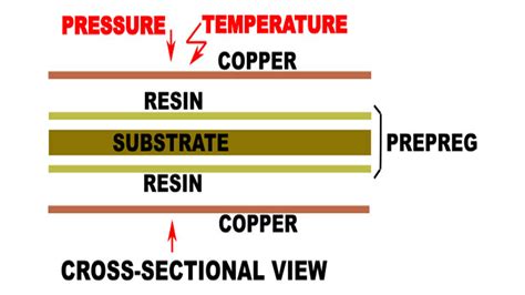
Applying the copper foil: The copper foil is placed on top of the dielectric substrate sheet, and the two layers are bonded together using heat and pressure. The bonding process typically involves a lamination press, which applies uniform pressure and temperature to ensure a strong and void-free bond between the copper foil and the substrate.
-
Curing: After lamination, the CCL undergoes a curing process to fully crosslink the epoxy resin in the dielectric substrate. This step improves the mechanical and thermal properties of the laminate.
-
Trimming and inspection: The cured CCL is trimmed to the desired size and shape, and the copper surface is cleaned and inspected for any defects or imperfections.

Electrical and Mechanical Properties of Copper Clad Laminate
The electrical and mechanical properties of CCL are critical to the performance and reliability of PCBs. Some of the key properties include:
Electrical Properties
-
Dielectric constant (Dk): The dielectric constant is a measure of the insulating material’s ability to store electrical energy. A lower Dk value indicates better signal integrity and higher signal speed. Typical Dk values for CCL range from 3.5 to 4.5.
-
Dissipation factor (Df): The dissipation factor is a measure of the dielectric material’s loss of electrical energy due to heat generation. A lower Df value indicates better signal integrity and lower power loss. Typical Df values for CCL range from 0.02 to 0.03.
-
Insulation resistance: Insulation resistance is a measure of the dielectric material’s ability to resist the flow of electrical current. A higher insulation resistance indicates better electrical insulation between conductive layers. Typical insulation resistance values for CCL are in the range of 10^6 to 10^8 MΩ.
Mechanical Properties
-
Flexural strength: Flexural strength is a measure of the laminate’s ability to resist bending and deformation under load. A higher flexural strength indicates better mechanical stability and durability. Typical flexural strength values for CCL range from 400 to 600 MPa.
-
Peel strength: Peel strength is a measure of the bond strength between the copper foil and the dielectric substrate. A higher peel strength indicates a more reliable and durable bond. Typical peel strength values for CCL range from 8 to 20 N/cm.
-
Glass transition temperature (Tg): The glass transition temperature is the temperature at which the dielectric material transitions from a rigid, glassy state to a soft, rubbery state. A higher Tg value indicates better thermal stability and the ability to withstand higher operating temperatures. Typical Tg values for CCL range from 130°C to 180°C.

Applications of Copper Clad Laminate
CCL is used in a wide range of applications across various industries. Some of the most common applications include:
-
Consumer electronics: CCL is used to manufacture PCBs for smartphones, tablets, laptops, televisions, and other consumer electronic devices.
-
Automotive: PCBs made from CCL are used in various automotive systems, such as engine control units, infotainment systems, and advanced driver assistance systems (ADAS).
-
Telecommunications: CCL is used in the production of PCBs for networking equipment, routers, switches, and cellular base stations.
-
Aerospace and defense: High-performance CCL, such as polyimide-based laminates, are used in the manufacturing of PCBs for aircraft, satellites, and military equipment.
-
Medical devices: CCL is used to create PCBs for medical devices, such as patient monitors, diagnostic equipment, and implantable devices.
-
Industrial automation: PCBs made from CCL are used in industrial control systems, sensors, and automation equipment.

Future Trends and Developments in Copper Clad Laminate Technology
As electronic devices continue to become more advanced and miniaturized, there is a growing demand for high-performance CCL materials that can support the increasing complexity and density of PCBs. Some of the future trends and developments in CCL technology include:
-
High-frequency materials: The development of CCL materials with lower dielectric constants and dissipation factors to support high-frequency applications, such as 5G wireless networks and millimeter-wave radar systems.
-
Thermally conductive materials: The incorporation of thermally conductive fillers, such as ceramic particles or graphene, into the dielectric substrate to improve heat dissipation and thermal management in high-power applications.
-
Flexible and stretchable laminates: The development of flexible and stretchable CCL materials to support the growing demand for flexible and wearable electronics.
-
Eco-friendly materials: The use of bio-based and recyclable materials in the production of CCL to reduce environmental impact and promote sustainability.
-
Additive manufacturing: The exploration of additive manufacturing techniques, such as 3D printing, to create customized and complex CCL structures for specific applications.
Frequently Asked Questions (FAQ)
-
What is the difference between single-sided and double-sided Copper Clad Laminate?
Single-sided CCL has a copper foil layer on one side of the dielectric substrate, while double-sided CCL has copper foil layers on both sides of the substrate. Double-sided CCL allows for the creation of more complex and compact PCB designs. -
How does the thickness of the copper foil affect the performance of the PCB?
The thickness of the copper foil determines the current-carrying capacity and the impedance of the conductive traces on the PCB. Thicker copper foil allows for higher current-carrying capacity and lower impedance, which is important for high-power and high-frequency applications. -
Can Copper Clad Laminate be recycled?
Yes, CCL can be recycled by separating the copper foil from the dielectric substrate using mechanical or chemical processes. The recovered copper can be reused in the production of new CCL or other copper-based products, while the dielectric substrate can be recycled into other materials or used as a fuel source in cement kilns. -
What is the shelf life of Copper Clad Laminate?
The shelf life of CCL depends on the storage conditions and the specific material composition. In general, CCL should be stored in a cool, dry place, away from direct sunlight and sources of heat or humidity. Under proper storage conditions, the shelf life of CCL can range from 6 months to 2 years. -
How do I choose the right Copper Clad Laminate for my application?
Choosing the right CCL for your application depends on several factors, including the electrical and mechanical requirements, the operating environment, and the cost constraints. Consider the dielectric constant, dissipation factor, thermal stability, and mechanical strength of the laminate, as well as the thickness and surface finish of the copper foil. Consult with CCL manufacturers or PCB design experts to select the most suitable material for your specific application.
In conclusion, Copper Clad Laminate is a crucial material in the production of printed circuit boards, serving as the foundation for creating conductive patterns that connect electronic components. The composition, structure, and properties of CCL play a vital role in determining the performance, reliability, and durability of PCBs across a wide range of applications. As electronic devices continue to advance and evolve, the development of new CCL materials and technologies will be essential to meet the growing demands of the industry and enable the creation of innovative and high-performance electronic products.
Leave a Reply