Introduction to AOI in PCB Manufacturing
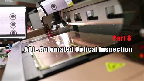
Automated Optical Inspection (AOI) is a critical process in the manufacturing of Printed Circuit Boards (PCBs). It is a non-contact method that uses advanced imaging technology to inspect the quality of PCBs during various stages of production. AOI systems are designed to detect and identify defects, ensuring that the final product meets the required quality standards.
In this article, we will explore the fundamentals of AOI in PCB manufacturing, its benefits, types of AOI systems, and the common defects it can detect. We will also discuss the advantages and limitations of AOI, and how it compares to other inspection methods.
The Importance of Quality Control in PCB Manufacturing
Quality control is paramount in PCB manufacturing, as even the smallest defect can lead to device malfunction or failure. PCBs are used in a wide range of applications, from consumer electronics to aerospace and military equipment. Any defect in these boards can have severe consequences, ranging from product recalls to safety hazards.
To ensure the highest quality standards, PCB manufacturers employ various inspection methods throughout the production process. These methods include:
- Visual inspection
- In-circuit testing (ICT)
- Flying probe testing
- Automated Optical Inspection (AOI)
Among these methods, AOI has gained significant popularity due to its speed, accuracy, and ability to detect a wide range of defects.

How Does AOI Work in PCB Inspection?
AOI systems use high-resolution cameras and advanced image processing algorithms to inspect PCBs. The process typically involves the following steps:
-
Image Acquisition: The AOI system captures high-resolution images of the PCB from various angles using specialized cameras.
-
Image Processing: The captured images are processed using advanced algorithms to enhance the image quality and highlight potential defects.
-
Defect Detection: The processed images are compared against a reference image or CAD data to identify any discrepancies or defects.
-
Defect Classification: The identified defects are classified based on their type, size, and location on the PCB.
-
Reporting: The AOI system generates a detailed report of the detected defects, which can be used for further analysis and corrective action.

Types of AOI Systems
There are three main types of AOI systems used in PCB manufacturing:
-
2D AOI: This system uses a single camera to capture 2D images of the PCB. It is suitable for inspecting surface-level defects such as solder bridging, component placement, and labeling errors.
-
3D AOI: This system uses multiple cameras or a combination of cameras and lasers to capture 3D images of the PCB. It can detect defects in component height, coplanarity, and solder joint quality.
-
Hybrid AOI: This system combines 2D and 3D inspection capabilities to provide a comprehensive inspection solution. It offers the benefits of both technologies, enabling the detection of a wide range of defects.

Common Defects Detected by AOI in PCBs
AOI systems can detect a variety of defects in PCBs, including:
- Component Placement Defects:
- Missing components
- Misaligned components
- Incorrect component polarity
-
Wrong component type
-
Solder Joint Defects:
- Solder bridging
- Insufficient solder
- Excess solder
-
Cold solder joints
-
Solder Paste Defects:
- Insufficient solder paste
- Excess solder paste
-
Solder paste contamination
-
Trace and Pad Defects:
- Broken traces
- Shorted traces
- Lifted pads
-
Contaminated pads
-
Other Defects:
- Labeling errors
- Dimensional discrepancies
- Fiducial mark issues
Advantages of AOI in PCB Manufacturing
AOI offers several advantages over other inspection methods in PCB manufacturing:
-
High Speed: AOI systems can inspect PCBs at a much faster rate compared to manual inspection, making it suitable for high-volume production.
-
Consistency: Unlike manual inspection, which is subject to human error and fatigue, AOI provides consistent and reliable results.
-
Early Defect Detection: AOI can be implemented at various stages of the production process, enabling early detection and correction of defects, reducing scrap and rework costs.
-
Wide Range of Defect Detection: AOI can detect a broad spectrum of defects, including those that may be difficult to identify through manual inspection.
-
Traceability: AOI systems generate detailed reports and store inspection data, providing traceability and facilitating continuous process improvement.
Limitations of AOI in PCB Inspection
Despite its numerous advantages, AOI has some limitations:
-
Initial Investment: Implementing an AOI system requires a significant initial investment in equipment and software.
-
Programming and Setup: AOI systems need to be programmed and set up for each specific PCB design, which can be time-consuming.
-
False Positives and False Negatives: AOI systems may occasionally generate false positives (identifying defects that do not exist) or false negatives (failing to detect actual defects).
-
Limited Subsurface Inspection: AOI primarily focuses on surface-level inspection and may not detect defects hidden beneath components or within the PCB layers.
Comparing AOI with Other Inspection Methods
| Inspection Method | Advantages | Disadvantages |
|---|---|---|
| Manual Inspection | – Low initial cost – Flexibility in inspection criteria |
– Slow and labor-intensive – Prone to human error and fatigue – Inconsistent results |
| In-Circuit Testing (ICT) | – Detects functional defects – Tests individual components |
– Requires custom fixtures – Limited coverage for dense PCBs – Potential for damage to PCBs |
| Flying Probe Testing | – No custom fixtures required – High test coverage – Suitable for low-volume production |
– Slower than ICT – Limited test access points – Higher cost compared to ICT |
| X-Ray Inspection | – Detects subsurface defects – Suitable for inspecting hidden joints |
– High equipment cost – Slower than AOI – Radiation safety concerns |
Best Practices for Implementing AOI in PCB Manufacturing
To maximize the benefits of AOI in PCB manufacturing, consider the following best practices:
-
Select the appropriate AOI system based on your specific requirements, such as PCB complexity, production volume, and defect types.
-
Develop a comprehensive inspection plan that defines the critical defects to be detected and the acceptable quality levels.
-
Ensure proper programming and setup of the AOI system for each PCB design, including the creation of accurate reference data.
-
Regularly calibrate and maintain the AOI system to ensure optimal performance and minimize false positives and false negatives.
-
Integrate AOI data with other quality control processes, such as statistical process control (SPC) and root cause analysis, for continuous improvement.
-
Provide adequate training to personnel involved in AOI operation, maintenance, and data analysis.
The Future of AOI in PCB Manufacturing
As PCB designs become more complex and miniaturized, the demand for advanced inspection solutions continues to grow. The future of AOI in PCB manufacturing is likely to be shaped by the following trends:
-
Integration of AI and Machine Learning: The incorporation of artificial intelligence (AI) and machine learning algorithms can enhance the accuracy and speed of defect detection and classification.
-
Inline AOI: Integrating AOI systems directly into the production line allows for real-time inspection and feedback, enabling faster correction of defects and reducing overall production time.
-
3D AOI Advancements: Continued advancements in 3D AOI technology, such as improved resolution and faster data processing, will enable the detection of more complex defects and enhance inspection efficiency.
-
Collaborative Robots (Cobots): The integration of AOI with collaborative robots can automate the handling and positioning of PCBs during inspection, further improving the speed and accuracy of the process.
Frequently Asked Questions (FAQ)
- What is the difference between 2D and 3D AOI systems?
-
2D AOI systems use a single camera to capture 2D images of the PCB, while 3D AOI systems use multiple cameras or a combination of cameras and lasers to capture 3D images. 3D AOI can detect defects in component height, coplanarity, and solder joint quality, which are not detectable by 2D AOI.
-
Can AOI replace manual inspection completely?
-
While AOI can significantly reduce the need for manual inspection, it may not replace it entirely. Some defects, such as those hidden beneath components or within the PCB layers, may still require manual inspection or other complementary methods like X-ray inspection.
-
How long does it take to set up an AOI system for a new PCB design?
-
The setup time for an AOI system varies depending on the complexity of the PCB design and the specific AOI software being used. It typically involves creating a reference image or CAD data, defining inspection parameters, and programming the system to detect the desired defects. The setup process can take several hours to a few days.
-
What factors should be considered when selecting an AOI system?
-
When selecting an AOI system, consider factors such as the complexity of your PCB designs, production volume, required defect detection capabilities, speed, accuracy, and budget. It is also essential to evaluate the ease of use, software features, and vendor support.
-
How often should an AOI system be calibrated?
- The frequency of calibration depends on the specific AOI system and the manufacturer’s recommendations. Generally, it is advisable to calibrate the system at regular intervals, such as monthly or quarterly, to ensure optimal performance. Additionally, calibration may be necessary after any major maintenance or software updates.
Conclusion
Automated Optical Inspection (AOI) has revolutionized quality control in PCB manufacturing. By providing fast, accurate, and consistent defect detection, AOI enables manufacturers to maintain high quality standards and reduce costs associated with scrap and rework.
As PCB designs continue to evolve and become more complex, the role of AOI in ensuring product quality will only grow in importance. By staying informed about the latest AOI technologies, best practices, and trends, PCB manufacturers can leverage this powerful tool to deliver reliable, high-quality products to their customers.
Leave a Reply