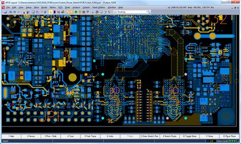
Plan Your PCB Layout Carefully
Create a Block Diagram First
Before starting your detailed PCB layout, it’s important to first create a high-level block diagram of your design. A block diagram will:
- Break the system down into major functional blocks
- Define the interfaces and connections between blocks
- Help visualize the overall architecture and data/power flow
Taking the time to plan out the block diagram will make the detailed PCB layout process go much smoother. It provides a roadmap to follow.
Consider PCB Layer Stack-Up
Give careful consideration to your PCB layer stack-up early in the design process. The number of layers and their arrangement will impact many aspects of the design.
Typical considerations when planning the layer stack-up include:
| Factor | Description |
|---|---|
| Signal integrity | More layers provide more routing flexibility to avoid crosstalk |
| Power integrity | Dedicated power/ground planes reduce impedance |
| EMI/EMC | Proper stack-up can help contain electromagnetic emissions |
| Manufacturing cost | Higher layer counts increase PCB fabrication cost |
A good starting point for many designs is a 4-layer board with a signal-ground-power-signal arrangement. This provides shielding between signal layers while keeping costs reasonable.
Floorplan Component Placement
With the layer stack-up determined, you can begin creating a floorplan for placing the major components on the board. Floorplanning involves:
- Arranging components to minimize sensitive signal routing lengths
- Providing adequate spacing to avoid thermal and EMI issues
- Ensuring sufficient board space for all required circuitry
- Positioning connectors, mounting holes, etc. for enclosure integration
Take the time to iterate on component placement until you achieve an optimized floorplan before proceeding to detailed routing. Moving components is much easier in the floorplanning stage vs. later on.
Follow Good Routing Practices
Minimize Sensitive Signal Trace Lengths
When routing your PCB, try to minimize the length of sensitive signal traces as much as possible. Sensitive signals include:
- High-speed signals (e.g. gigabit transceivers)
- Precise analog signals
- Clock signals
- Antenna feed lines
Excessive trace lengths can degrade signal integrity and cause issues like:
| Issue | Potential Impact |
|---|---|
| Attenuation | Reduced signal strength at receiver |
| Reflections | Signal distortion, false triggering |
| Crosstalk | Interference from nearby signal traces |
| EMI radiation | Failing emissions tests, interference |
Where long signal traces can’t be avoided, consider using thicker traces, spacing them further from other signals, or using shielding.
Route Power and Ground First
When starting to route your PCB, it’s generally best to route the power and ground nets first before signal traces. Benefits of routing power/ground first include:
- Ensuring low-impedance paths for power distribution
- Avoiding signal traces blocking power routing channels
- Minimizing loops that could cause EMI radiation
Use thick traces and dedicated power/ground planes in your stack-up where possible to keep impedance low. Also use multiple vias when transitioning between layers to reduce inductance.
Carefully Terminate High-Speed Signals
High-speed signals require proper termination at the source and/or load to maintain signal integrity. Termination is used to:
- Match trace impedance to driver/receiver
- Absorb reflections to avoid ringing and distortion
- Reduce EMI radiation
The appropriate termination style depends on the signaling standard being used. Common termination styles include:
| Style | Usage |
|---|---|
| Series | Source-terminated point-to-point links |
| Parallel | Distributed loads, bi-directional buses |
| AC | Capacitive coupling, removing DC offsets |
Failing to properly terminate high-speed signals is a common source of signal integrity and EMI issues in PCB designs. Be sure to carefully review termination requirements.

Implement Robust Power Distribution
Use Appropriate Decoupling Capacitors
Decoupling capacitors are critical for providing clean, stable power to ICs and preventing power supply noise from coupling into sensitive signals. Some key considerations for decoupling capacitors include:
- Place as close to IC power pins as possible to minimize inductance
- Use multiple capacitors in parallel (e.g. 0.1uF, 0.01uF, 0.001uF)
- Size capacitors appropriately based on current draw and slew rate
- Use low-ESR and low-ESL capacitor types
Be sure to place decoupling capacitors for every power pin on an IC. Also provide bulk decoupling capacitors (e.g. 10-100uF) near voltage regulators to smooth the output.
Define Proper Power Plane Cuts
On PCBs with dedicated power and ground planes, you’ll often need to make cuts in the planes to avoid coupling between different voltage rails. Some plane cut guidelines include:
- Physically separate different supply voltages to prevent shorts
- Provide a continuous ground plane – avoid splits where possible
- Keep high current planes (e.g. 3.3V, 5V) away from sensitive planes (e.g. 1.8V)
- Use thin neck-downs vs. abrupt plane cuts to avoid impedance discontinuities
Proper floor planning of your voltage rails on the power plane layer(s) will help ensure a robust power distribution network. Simulate the PDN if needed to verify performance.

Carefully Review Manufacturability
Follow the Fabricator’s DFM Guidelines
Before sending your PCB design out for fabrication, be sure to carefully review the fabricator’s design for manufacturing (DFM) guidelines. Typical DFM guidelines include:
- Minimum trace width and spacing by copper weight
- Minimum hole size and annular ring
- Minimum soldermask webbing and clearances
- Panelization and tooling hole requirements
Failing to follow the fab shop’s DFM guidelines can result in your design being rejected for manufacture. This causes delays and potentially increases costs if re-design is required.
Perform Design Rule Checks
In addition to manual DFM reviews, be sure to leverage your PCB CAD tools to perform automated design rule checking (DRC). DRC will verify your design meets rules like:
- Minimum trace width and clearances are met
- Vias are sized appropriately and not too close to traces/pads
- Copper pours have proper isolation from other nets
- Drill holes meet sizing and placement criteria
Configure your DRC settings to meet the fab shop’s capabilities and run the checks periodically as you work on the design. Don’t wait until the design is complete to run DRC.

Optimize for Assembly and Test
Provide Adequate Space for Assembly
In addition to making the PCB fabricatable, you also need to ensure it can be easily assembled. Provide adequate space around components for pick-and-place machines and soldering equipment.
Some typical rules of thumb for component spacing include:
| Component Type | Spacing |
|---|---|
| Passive (0201 and larger) | 0.15-0.2 mm |
| Passive (01005) | 0.1-0.15 mm |
| Fine pitch leaded | 0.2-0.25 mm (lead tip to tip) |
| BGAs | 0.5-1 mm (depending on ball pitch) |
Consult with your contract manufacturer (CM) to understand their specific assembly requirements. Provide the CM the centroid data file to assist with assembly planning.
Include Testpoints and Probe Access
To facilitate testing your PCB for proper functionality, be sure to include adequate test points and probe access. Some test access tips include:
- Provide test points for critical signal, power and ground nets
- Ensure test points are accessible for probing (not under components)
- Include unmasked vias/pads for bed-of-nails or flying probe test access
- Provide an unmasked ground point near analog test points
Work with your CM to define what test points are required to verify the PCB in production. Well designed test access will make debug and failure analysis much easier.
Frequently Asked Questions (FAQ)
What is the best PCB design software?
There are many excellent PCB design tools on the market, both free/open-source and commercial. Some of the most popular options include:
- KiCad (open source)
- Eagle (entry-level commercial)
- Altium Designer (full-featured commercial)
- OrCad/Allegro (full-featured commercial)
The “best” option depends on your specific needs and budget. It’s worth evaluating a few options before committing to one toolset.
How many layers should my PCB have?
The number of layers your PCB needs depends on several factors, including:
- Complexity of the circuit (package density, pin count)
- Signal integrity requirements (layer shielding, impedance control)
- Power integrity (dedicated power/ground planes)
- Cost and time-to-market targets
A good starting point for many designs is a 4-layer board with signal-power-ground-signal arrangement. This provides good signal integrity and routability while keeping costs reasonable.
Simple designs can often use a 2-layer PCB. Very complex designs may require 6, 8 or even 12+ layers. Work with your manufacturer to determine the most appropriate layer count.
What is a good trace width and clearance to use?
Trace width and clearance depends on several factors, like:
- Current carrying requirements (wider traces for more current)
- Voltage (higher voltage requires more clearance)
- Manufacturing capabilities (smaller width/clearance costs more)
- Available board space (less space requires thinner traces)
For low-voltage, low-current signals, 0.1-0.15 mm trace width and clearance is typically a good starting point. For power traces, use a trace width calculator to size for current.
Always consult with your PCB fabricator for their specific trace width and clearance capabilities. Avoid pushing the limits of the process if possible.
How do I reduce EMI in my PCB?
Some tips for reducing electromagnetic interference (EMI) in PCB designs include:
- Use solid power and ground planes for shielding
- Route high-speed signals on inner layers between planes
- Keep loop areas small (short traces, decoupling capacitors close to ICs)
- Use guard rings/traces around sensitive analog circuitry
- Provide filtering on signal and power lines entering/exiting the PCB
At the end of the day, reducing EMI requires minimizing current loops that can radiate fields. Careful design partitioning and stack-up are key for avoiding EMI issues.
Should I panelize my PCB?
Panelizing your PCB can offer several benefits, including:
- Reduced handling time (fabrication, assembly, testing)
- Shared tooling costs across multiple copies of a design
- Easier tracking and kitting of boards that go together
Panelization does add some restrictions on the design – need to account for panel size, rail clearances, fiducials, etc. It can also somewhat limit your fab shop options.
For prototypes and small volumes, going with individually routed PCBs is usually the most cost effective. As volumes increase, the benefits of panelization start to become worthwhile.
Leave a Reply