Understanding Least-Impedance Return Paths
In the world of PCB design, creating efficient and reliable return paths is crucial for ensuring the proper functioning of electronic devices. One key concept that designers must grasp is the idea of least-impedance return paths. By understanding and implementing this principle, designers can create PCBs that minimize signal distortion, reduce electromagnetic interference (EMI), and improve overall system performance.
What are Return Paths?
Return paths are the routes that electrical currents take to complete a circuit. In a PCB, these paths are typically formed by the ground or power planes, which provide a low-impedance connection between components. When a signal travels from one point to another on a PCB, it must have a corresponding return path to maintain signal integrity and prevent unwanted radiation.
The Importance of Least-Impedance Return Paths
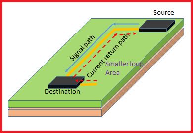
The concept of least-impedance return paths is based on the fact that electrical currents always follow the path of least resistance. In a PCB, this means that return currents will naturally flow along the path with the lowest impedance. By designing return paths that follow the least-impedance route, designers can ensure that signals remain clean and undistorted, while also minimizing EMI and crosstalk between adjacent traces.
Designing PCBs with Least-Impedance Return Paths
Proper Grounding Techniques
One of the most important aspects of creating least-impedance return paths is implementing proper grounding techniques. This involves using ground planes, which are large copper areas that provide a low-impedance connection between components. By placing ground planes close to signal traces, designers can minimize the loop area between the signal and its return path, reducing inductance and improving signal integrity.
Ground Plane Placement
| Layer | Purpose |
|---|---|
| Top | Signal traces, components |
| Inner 1 | Ground plane |
| Inner 2 | Power plane |
| Bottom | Signal traces, components |
When designing a PCB, it’s essential to place ground planes as close as possible to the signal layers. In a typical four-layer board, the inner layers are often dedicated to ground and power planes, while the outer layers are used for signal traces and components. This arrangement minimizes the distance between signals and their return paths, reducing inductance and improving signal quality.
Avoiding Discontinuities in Return Paths
Another crucial aspect of designing least-impedance return paths is avoiding discontinuities in the ground plane. Discontinuities, such as slots or gaps in the ground plane, can cause return currents to deviate from their intended path, leading to signal distortion and increased EMI. To minimize these issues, designers should maintain a continuous ground plane whenever possible and use stitching vias to connect ground planes on different layers.
Stitching Vias
Stitching vias are small, closely-spaced vias that connect ground planes on different layers of a PCB. By providing multiple low-impedance paths between layers, stitching vias help maintain the integrity of return paths and reduce the impact of discontinuities in the ground plane.
Routing Techniques for Least-Impedance Return Paths
Proper routing techniques are also essential for creating least-impedance return paths. When routing signal traces, designers should follow these guidelines:
- Route signals over continuous ground planes whenever possible
- Avoid routing signals over gaps or slots in the ground plane
- Use ground stitching vias near signal vias to maintain return path continuity
- Minimize the distance between signal traces and their corresponding return paths
By adhering to these routing techniques, designers can ensure that return currents follow the path of least impedance, minimizing signal distortion and EMI.

Benefits of Least-Impedance Return Paths
Designing PCBs with least-impedance return paths offers several key benefits:
-
Improved signal integrity: By minimizing the distance between signals and their return paths, least-impedance return paths reduce inductance and signal distortion, resulting in cleaner, more reliable signals.
-
Reduced EMI: Least-impedance return paths help confine electromagnetic fields close to the PCB surface, minimizing radiation and reducing the likelihood of EMI issues.
-
Better power integrity: Properly designed return paths ensure that power is efficiently distributed throughout the PCB, reducing voltage drops and improving overall system performance.
-
Increased reliability: By minimizing signal distortion and EMI, least-impedance return paths contribute to the overall reliability and longevity of electronic devices.

Common Mistakes to Avoid
When designing PCBs with least-impedance return paths, there are several common mistakes that designers should avoid:
-
Neglecting the importance of ground planes: Failing to include adequate ground planes can lead to poor signal integrity and increased EMI.
-
Creating discontinuities in the ground plane: Gaps or slots in the ground plane can cause return currents to deviate from their intended path, resulting in signal distortion and EMI issues.
-
Routing signals over gaps or slots: Routing signals over discontinuities in the ground plane can disrupt return paths and degrade signal quality.
-
Ignoring the need for ground stitching vias: Neglecting to use stitching vias can lead to poor connections between ground planes on different layers, compromising the integrity of return paths.
By being aware of these common mistakes and taking steps to avoid them, designers can create PCBs with optimal return paths that ensure reliable performance.

Frequently Asked Questions (FAQ)
-
What is the importance of return paths in PCB design?
Return paths are essential for maintaining signal integrity, minimizing EMI, and ensuring proper power distribution in a PCB. Without well-designed return paths, signals can become distorted, leading to poor performance and reliability issues. -
How do least-impedance return paths benefit PCB design?
Least-impedance return paths benefit PCB design by minimizing signal distortion, reducing EMI, improving power integrity, and increasing overall system reliability. By ensuring that return currents follow the path of least resistance, designers can create PCBs that perform optimally and meet stringent performance requirements. -
What role do ground planes play in creating least-impedance return paths?
Ground planes are crucial for creating least-impedance return paths in a PCB. By providing a low-impedance connection between components, ground planes help minimize the loop area between signals and their return paths, reducing inductance and improving signal integrity. Placing ground planes close to signal layers is essential for optimal performance. -
How can designers avoid discontinuities in return paths?
To avoid discontinuities in return paths, designers should maintain a continuous ground plane whenever possible and use stitching vias to connect ground planes on different layers. Avoiding routing signals over gaps or slots in the ground plane is also essential for maintaining return path integrity. -
What are some common mistakes to avoid when designing least-impedance return paths?
Common mistakes to avoid when designing least-impedance return paths include neglecting the importance of ground planes, creating discontinuities in the ground plane, routing signals over gaps or slots, and ignoring the need for ground stitching vias. By being aware of these pitfalls and taking steps to avoid them, designers can create PCBs with optimal return paths.
Conclusion
Designing PCBs with least-impedance return paths is essential for ensuring reliable, high-performance electronic devices. By understanding the principles behind least-impedance return paths and implementing proper grounding techniques, avoiding discontinuities, and following best practices for routing, designers can create PCBs that minimize signal distortion, reduce EMI, and improve overall system performance. As the demand for faster, more complex electronic systems continues to grow, mastering the art of designing least-impedance return paths will become increasingly critical for PCB designers looking to stay ahead of the curve.
Leave a Reply