Introduction to PCB UV-Lasers
Printed Circuit Boards (PCBs) are the backbone of modern electronics, found in everything from smartphones to aerospace systems. The manufacturing process of PCBs has evolved significantly over the years, with new technologies constantly emerging to improve efficiency, precision, and reliability. One such technology that has gained prominence in recent years is the use of ultraviolet (UV) lasers in PCB manufacturing.
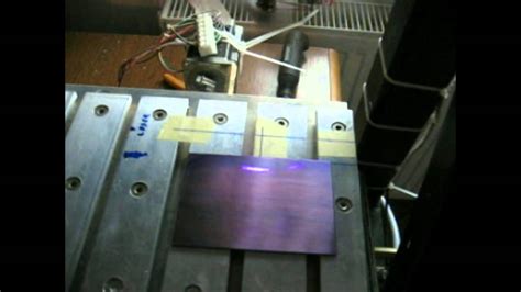
UV lasers have become an essential tool in the PCB industry due to their ability to perform high-precision drilling, cutting, and patterning of various materials used in PCB fabrication. These lasers operate in the ultraviolet spectrum, typically at wavelengths between 350 and 400 nanometers, which allows for smaller focused spot sizes and higher energy densities compared to traditional infrared lasers.
Advantages of UV Lasers in PCB Manufacturing
- High precision: UV lasers can achieve spot sizes as small as 10 microns, enabling the creation of ultra-fine features and micro-vias on PCBs.
- Reduced thermal damage: The shorter wavelength of UV lasers results in lower heat transfer to surrounding areas, minimizing thermal damage to the PCB substrate.
- Increased processing speed: UV lasers can operate at higher frequencies and scanning speeds, leading to faster processing times and higher throughput.
- Versatility: UV lasers can process a wide range of materials used in PCB manufacturing, including copper, dielectrics, and solder masks.
Applications of UV Lasers in PCB Manufacturing
Drilling and Via Formation
One of the primary applications of UV lasers in PCB manufacturing is the drilling of micro-vias and through-holes. Micro-vias are small, blind holes that connect inner layers of a multi-layer PCB, while through-holes penetrate the entire thickness of the board. UV lasers can create these features with high precision and minimal damage to the surrounding material.
The process involves focusing the UV laser beam onto the desired location on the PCB and pulsing the laser to ablate the material. The laser parameters, such as pulse duration, energy, and repetition rate, are carefully controlled to achieve the desired hole size and depth. UV lasers can drill holes as small as 25 microns in diameter, which is essential for high-density interconnect (HDI) PCBs used in advanced electronic devices.
Patterning and Selective Removal
UV lasers are also used for patterning and selective removal of materials on PCBs. This process is known as laser direct imaging (LDI) and involves using the laser to directly expose a photoresist layer on the PCB, creating the desired circuit pattern. LDI eliminates the need for traditional photolithography masks, reducing costs and increasing flexibility in PCB design.
In addition to patterning, UV lasers can selectively remove materials such as solder masks, dielectric layers, and copper. This process, called laser skiving, is used to create openings in solder masks for component pads, expose copper traces for electrical testing, and remove dielectric materials for via formation.
Cutting and Singulation
UV lasers are increasingly being used for cutting and singulation of PCBs. Singulation is the process of separating individual PCBs from a larger panel after the manufacturing process is complete. Traditionally, this was done using mechanical methods such as routing or punching, which can cause stress and damage to the PCBs.
UV laser cutting offers a non-contact, stress-free alternative for PCB singulation. The laser can cut through the PCB substrate, copper layers, and solder masks with high precision and minimal debris. This results in cleaner, burr-free edges and reduced risk of delamination or cracking.

UV Laser Technology
Types of UV Lasers
There are several types of UV lasers used in PCB manufacturing, each with its own characteristics and advantages.
-
Excimer Lasers: These lasers use a combination of a noble gas (such as argon, krypton, or xenon) and a halogen (such as fluorine or chlorine) to generate UV light. Common excimer lasers used in PCB manufacturing include KrF (248 nm) and XeF (351 nm) lasers. Excimer lasers offer high pulse energies and can process a wide range of materials, but they have a relatively large footprint and high operating costs.
-
Diode-Pumped Solid-State (DPSS) Lasers: DPSS lasers use a diode laser to pump a solid-state gain medium, such as neodymium-doped yttrium orthovanadate (Nd:YVO4) or neodymium-doped yttrium aluminum garnet (Nd:YAG). The output of the gain medium is then frequency-tripled or quadrupled to achieve UV wavelengths. Common UV DPSS lasers include 355 nm (Nd:YVO4) and 266 nm (Nd:YAG) lasers. DPSS lasers offer high efficiency, excellent beam quality, and a compact footprint, making them popular for PCB manufacturing applications.
-
Fiber Lasers: UV fiber lasers use a fiber doped with rare-earth elements, such as erbium or ytterbium, as the gain medium. The output of the fiber laser is frequency-converted to UV wavelengths using nonlinear optical crystals. UV fiber lasers offer high efficiency, excellent beam quality, and a compact, rugged design, making them suitable for industrial environments.
Laser Parameters
The performance of UV lasers in PCB manufacturing depends on several key parameters:
-
Wavelength: The wavelength of the UV laser determines the absorption characteristics of the material being processed. Shorter wavelengths generally result in higher absorption and better resolution.
-
Pulse Duration: The pulse duration of the laser affects the amount of heat transferred to the material and the precision of the process. Shorter pulse durations (in the nanosecond or picosecond range) result in less thermal damage and higher precision.
-
Power and Energy: The power and energy of the laser determine the rate at which material is removed and the processing speed. Higher powers and energies allow for faster processing but may also increase the risk of thermal damage.
-
Beam Quality: The beam quality of the laser affects the focused spot size and the precision of the process. Higher beam quality (lower M2 value) results in smaller spot sizes and better resolution.
Laser System Components
A typical UV laser system for PCB manufacturing consists of several key components:
-
Laser Source: The UV laser source generates the laser beam with the desired wavelength and pulse characteristics.
-
Beam Delivery System: The beam delivery system includes mirrors, lenses, and other optical components that guide and focus the laser beam onto the PCB surface.
-
Scanning System: The scanning system, such as a galvanometer or a linear motor, moves the laser beam across the PCB surface to create the desired pattern or feature.
-
Vision System: A vision system, such as a camera or a microscope, is used to align the PCB and inspect the processed features for quality control.
-
Control Software: The control software coordinates the operation of the laser, scanning, and vision systems and allows the operator to set process parameters and monitor the system performance.

Process Optimization and Quality Control
To achieve the best results with UV lasers in PCB manufacturing, it is essential to optimize the process parameters and implement robust quality control measures.
Process Optimization
Process optimization involves selecting the appropriate laser parameters, such as wavelength, pulse duration, power, and scanning speed, for each specific application and material. This requires a thorough understanding of the material properties, such as absorption characteristics, thermal conductivity, and ablation threshold.
Empirical testing and statistical analysis are often used to determine the optimal process window for each application. Design of Experiments (DoE) techniques, such as factorial designs or response surface methodology, can help identify the most critical parameters and their interactions.
Process simulation and modeling tools, such as finite element analysis (FEA) or computational fluid dynamics (CFD), can also be used to predict the laser-material interaction and optimize the process parameters. These tools can help reduce the need for extensive experimental trials and accelerate the development of new applications.
Quality Control
Quality control is crucial to ensure that the PCBs processed with UV lasers meet the required specifications and performance criteria. Several methods are used to assess the quality of laser-processed PCBs:
-
Visual Inspection: Visual inspection, either manual or automated, is used to check for surface defects, such as burns, discoloration, or debris.
-
Dimensional Measurement: Dimensional measurement techniques, such as optical microscopy or scanning electron microscopy (SEM), are used to verify the size, shape, and position of laser-drilled holes, vias, and other features.
-
Electrical Testing: Electrical testing, such as continuity or insulation resistance tests, is performed to ensure that the laser-processed PCBs meet the required electrical performance specifications.
-
Cross-Sectional Analysis: Cross-sectional analysis, using techniques such as grinding or ion beam milling, is used to examine the internal structure of the PCB and verify the integrity of the laser-drilled vias and interconnects.
Implementing statistical process control (SPC) methods, such as control charts or process capability analysis, can help monitor the process stability and identify potential issues before they affect the final product quality.

Future Trends and Developments
As the demand for higher density, higher performance PCBs continues to grow, the use of UV lasers in PCB manufacturing is expected to expand further. Several emerging trends and developments are shaping the future of this technology:
-
Shorter Wavelengths: The development of UV lasers with shorter wavelengths, such as 193 nm or even extreme UV (EUV) wavelengths, can enable the creation of even smaller features and higher resolution patterns on PCBs.
-
Ultrafast Lasers: The use of ultrafast lasers, with pulse durations in the picosecond or femtosecond range, can reduce thermal damage and improve the precision of the laser processing.
-
Hybrid Processes: Combining UV laser processing with other technologies, such as inkjet printing or additive manufacturing, can enable the creation of novel PCB structures and functionalities.
-
Flexible Electronics: UV lasers can play a critical role in the manufacturing of flexible and stretchable PCBs, which are increasingly being used in wearable devices, medical implants, and other emerging applications.
-
Sustainability: The development of more energy-efficient and environmentally friendly UV laser systems, as well as the use of biodegradable or recyclable PCB materials, can contribute to the sustainability of the electronics industry.
Frequently Asked Questions (FAQ)
-
What are the main advantages of using UV lasers in PCB manufacturing?
UV lasers offer several advantages in PCB manufacturing, including high precision, reduced thermal damage, increased processing speed, and versatility in processing a wide range of materials. -
What are the typical applications of UV lasers in PCB manufacturing?
UV lasers are commonly used for drilling micro-vias and through-holes, patterning and selective removal of materials (laser direct imaging and laser skiving), and cutting and singulation of PCBs. -
What types of UV lasers are used in PCB manufacturing?
The main types of UV lasers used in PCB manufacturing are excimer lasers (KrF and XeF), diode-pumped solid-state lasers (Nd:YVO4 and Nd:YAG), and UV fiber lasers. -
How can process optimization be achieved for UV laser PCB manufacturing?
Process optimization involves selecting the appropriate laser parameters, such as wavelength, pulse duration, power, and scanning speed, for each specific application and material. Empirical testing, statistical analysis, and simulation tools can be used to determine the optimal process window. -
What are some future trends and developments in UV laser PCB manufacturing?
Future trends and developments in UV laser PCB manufacturing include the use of shorter wavelengths, ultrafast lasers, hybrid processes, flexible electronics, and sustainable manufacturing practices.
Conclusion
UV lasers have revolutionized the PCB manufacturing industry, offering high precision, flexibility, and efficiency in the creation of advanced electronic devices. As the technology continues to evolve, with new laser sources, shorter wavelengths, and ultrafast pulses, the capabilities of UV lasers in PCB manufacturing will only expand further.
However, the successful implementation of UV lasers in PCB manufacturing requires a deep understanding of the laser-material interaction, process optimization, and quality control. Close collaboration between laser manufacturers, PCB designers, and end-users is essential to unlock the full potential of this technology and address the challenges of the rapidly evolving electronics industry.
As we look to the future, UV lasers will undoubtedly play a crucial role in enabling the next generation of PCBs, from high-density interconnects for 5G networks to flexible and stretchable electronics for wearable devices. By embracing this technology and investing in research and development, the PCB industry can stay at the forefront of innovation and meet the demands of an increasingly connected world.
Leave a Reply