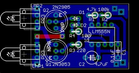
What is PCB Silkscreen Printing?
PCB silkscreen printing is a process used in the manufacturing of printed circuit boards to apply text, logos, and other markings onto the surface of the PCB. The silkscreen process involves using a fine mesh screen, typically made of polyester or stainless steel, to transfer ink onto the PCB surface. The screen has a stencil of the desired design, and when ink is pushed through the mesh, it creates a precise image on the PCB.
Silkscreen printing is an essential step in PCB manufacturing as it provides important information for assembly, testing, and troubleshooting. Some common applications of silkscreen printing on PCBs include:
- Component labels and values
- Company logos and product branding
- Test points and fiducial markers
- Warning and safety information
- Barcodes and serial numbers
Advantages of Silkscreen Printing
Silkscreen printing offers several advantages over other marking methods, such as:
- Durability: Silkscreen ink is designed to withstand the harsh conditions of PCB assembly and use, such as high temperatures and exposure to solvents.
- Precision: The fine mesh screen allows for high-resolution printing of small, detailed designs.
- Efficiency: Silkscreen printing is a fast and cost-effective method for marking large quantities of PCBs.
- Versatility: Silkscreen ink is available in a variety of colors and can be used on different PCB surface finishes, such as HASL, ENIG, and OSP.
Silkscreen Printing Process
The silkscreen printing process involves several steps:
- Screen Preparation: A stencil of the desired design is created on the mesh screen using a photosensitive emulsion. The emulsion is exposed to light, hardening the areas that will not be printed.
- Ink Preparation: The silkscreen ink is mixed and loaded onto the screen.
- Printing: The PCB is placed under the screen, and a squeegee is used to push the ink through the mesh onto the PCB surface.
- Curing: The printed PCB is then heated to cure the ink, making it permanent and durable.
Silkscreen Ink Types
There are two main types of silkscreen ink used in PCB manufacturing:
-
Epoxy-Based Ink: This type of ink is the most common and offers excellent durability, adhesion, and resistance to chemicals and abrasion. Epoxy-based ink requires curing at high temperatures (around 150°C) for optimal performance.
-
UV-Curable Ink: This type of ink is cured using ultraviolet light, which allows for faster processing times and lower energy consumption compared to epoxy-based ink. UV-curable ink is ideal for applications that require a quick turnaround or have temperature-sensitive components.
The choice of ink depends on the specific requirements of the PCB, such as the surface finish, environmental conditions, and production timeline.

Design Considerations for PCB Silkscreen
When designing the silkscreen layout for a PCB, there are several factors to consider:
-
Legibility: The text and symbols should be clear and easy to read, with appropriate font sizes and styles. A minimum font size of 0.8mm is recommended for standard designs.
-
Contrast: The ink color should provide sufficient contrast against the PCB surface finish for optimal legibility. White ink is the most common choice for dark surfaces, while black ink is used for lighter surfaces.
-
Placement: The silkscreen design should not interfere with the function of the PCB components or test points. Adequate clearance should be maintained around pads, vias, and other features.
-
Consistency: The silkscreen layout should be consistent across the entire PCB design, with uniform font sizes, styles, and orientations.
-
Manufacturing Limitations: The silkscreen design should take into account the limitations of the manufacturing process, such as minimum line widths and spacing.
Here is a table summarizing the recommended minimum dimensions for PCB silkscreen designs:
| Feature | Minimum Dimension |
|---|---|
| Line Width | 0.15mm |
| Space Between Lines | 0.15mm |
| Font Size | 0.8mm |
| Space Between Characters | 0.15mm |
| Space Between Words | 0.3mm |

Common Silkscreen Printing Issues and Solutions
Despite the advantages of silkscreen printing, there are several common issues that can arise during the process:
-
Incomplete or Inconsistent Coverage: This can be caused by a clogged screen, insufficient ink, or improper squeegee pressure. Regular screen maintenance, proper ink preparation, and operator training can help prevent this issue.
-
Smudging or Bleeding: This can occur if the ink is too thin or the PCB surface is contaminated. Using the appropriate ink viscosity and ensuring a clean PCB surface can mitigate this problem.
-
Poor Adhesion: This can result from incompatible ink, inadequate curing, or surface contamination. Selecting the proper ink for the PCB surface finish and following the recommended curing process can improve adhesion.
-
Misalignment: This can happen if the screen is not properly aligned with the PCB or if the PCB moves during printing. Using alignment fixtures and proper operator technique can ensure accurate registration.
-
Damaged or Worn Screens: Over time, the mesh screen can become stretched or torn, leading to poor print quality. Regular screen inspection and replacement can prevent this issue.

Alternatives to Silkscreen Printing
While silkscreen printing is the most common method for marking PCBs, there are several alternatives:
-
Direct Inkjet Printing: This method uses a digital inkjet printer to apply the design directly onto the PCB surface. Inkjet printing offers greater flexibility and faster setup times compared to silkscreen printing but may not be as durable.
-
Laser Marking: This process uses a laser to etch the design onto the PCB surface. Laser marking is permanent and highly precise but can be more expensive than silkscreen printing.
-
Pad Printing: This method uses a silicone pad to transfer the ink from a cliché onto the PCB surface. Pad printing is suitable for irregular surfaces and fine details but may not be as efficient for large quantities.
-
Labeling: Pre-printed labels can be applied to the PCB surface as an alternative to direct printing. Labels offer flexibility and can be easily removed or replaced but may not be as durable as direct printing methods.
The choice of marking method depends on the specific requirements of the PCB, such as durability, precision, cost, and production volume.
Frequently Asked Questions (FAQ)
- What is the minimum font size for PCB silkscreen printing?
-
The recommended minimum font size for standard PCB silkscreen designs is 0.8mm. This ensures adequate legibility for text and symbols.
-
Can silkscreen ink be removed from a PCB?
-
Silkscreen ink is designed to be permanent and durable, so it cannot be easily removed without damaging the PCB surface. In some cases, specialized solvents or abrasive methods may be used for removal, but this is not recommended as it can affect the PCB functionality.
-
How long does silkscreen ink take to cure?
-
The curing time for silkscreen ink depends on the type of ink and the curing method. Epoxy-based ink typically requires curing at high temperatures (around 150°C) for 30-60 minutes. UV-curable ink can be cured in a matter of seconds using ultraviolet light.
-
Can silkscreen printing be used on flexible PCBs?
-
Yes, silkscreen printing can be used on flexible PCBs, but the process may require specialized equipment and ink formulations to accommodate the unique properties of flexible substrates. The ink must be able to flex with the PCB without cracking or losing adhesion.
-
What is the maximum number of colors that can be used in PCB silkscreen printing?
- In theory, there is no limit to the number of colors that can be used in PCB silkscreen printing, as each color requires a separate screen and printing pass. However, in practice, most PCB designs use only one or two colors (typically white and/or black) to maintain legibility and cost-effectiveness. Multiple colors may be used for specialized applications or custom designs.
In conclusion, PCB silkscreen printing is a crucial process in the manufacturing of printed circuit boards, providing essential information for assembly, testing, and troubleshooting. By understanding the silkscreen printing process, ink types, design considerations, and common issues, PCB designers and manufacturers can ensure high-quality, durable, and legible markings on their products. As technology advances, alternative marking methods may offer new possibilities, but silkscreen printing remains the industry standard for its versatility, efficiency, and reliability.
Leave a Reply