What is an ENIG Test Pad?
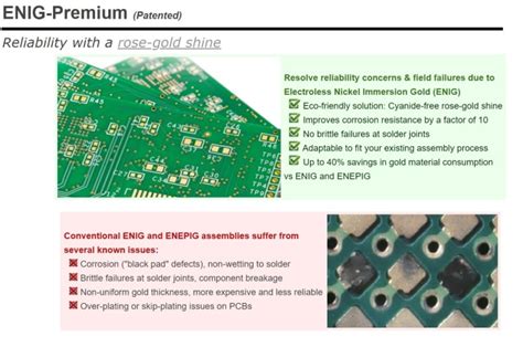
An ENIG (Electroless Nickel Immersion Gold) test pad is a specialized type of pad used in printed circuit board (PCB) manufacturing for testing purposes. These pads are plated with a layer of nickel followed by a thin layer of gold, which provides excellent oxidation resistance and enhances the solderability of the pad. ENIG test pads are commonly used for testing the continuity, resistance, and overall functionality of the PCB.
Advantages of ENIG Test Pads
- Enhanced solderability
- Excellent oxidation resistance
- Compatibility with a wide range of soldering processes
- Improved shelf life of the PCB
- Better electrical conductivity compared to other surface finishes
ENIG Test Pad Manufacturing Process
The manufacturing process of ENIG test pads involves several steps:
-
Copper Plating: The test pad area is plated with a layer of copper, which serves as the base for the subsequent layers.
-
Nickel Plating: A layer of nickel is then deposited onto the copper layer using an electroless plating process. The nickel layer acts as a barrier, preventing the diffusion of copper into the gold layer.
-
Gold Plating: Finally, a thin layer of gold is deposited onto the nickel layer through an immersion process. The gold layer provides excellent oxidation resistance and enhances the solderability of the test pad.
| Step | Process | Purpose |
|---|---|---|
| 1 | Copper Plating | Serves as the base layer |
| 2 | Nickel Plating | Acts as a barrier layer |
| 3 | Gold Plating | Provides oxidation resistance and enhances solderability |
ENIG Test Pad With Solder Paste
When using ENIG test pads with solder paste, there are several factors to consider to ensure optimal performance and reliability.
Solder Paste Selection
Choosing the right solder paste is crucial when working with ENIG test pads. The solder paste should be compatible with the surface finish of the test pad and the soldering process being used. Some key factors to consider when selecting a solder paste include:
- Alloy composition
- Particle size
- Flux type
- Viscosity
Stencil Design
The stencil design plays a critical role in the application of solder paste onto ENIG test pads. The aperture size and shape should be optimized to ensure the proper amount of solder paste is deposited onto the test pad. Factors to consider when designing the stencil include:
- Aperture size and shape
- Stencil thickness
- Aperture wall angle
- Stencil material
Reflow Profile
The reflow profile is another important consideration when using ENIG test pads with solder paste. The reflow profile should be optimized to ensure proper wetting of the solder paste onto the test pad and to minimize the formation of voids or other defects. Key factors to consider when developing the reflow profile include:
- Peak temperature
- Time above liquidus
- Ramp rates
- Cooling rate

ENIG Test Pad Without Solder Paste
In some cases, ENIG test pads may be used without solder paste, particularly when testing the continuity or resistance of the PCB. When using ENIG test pads without solder paste, there are several factors to consider to ensure accurate and reliable test results.
Probe Selection
Choosing the right probe is essential when testing ENIG test pads without solder paste. The probe should be compatible with the surface finish of the test pad and should provide reliable contact with the pad surface. Some key factors to consider when selecting a probe include:
- Probe tip material
- Probe tip shape and size
- Spring force
- Current carrying capacity
Test Fixture Design
The test fixture design is another important consideration when using ENIG test pads without solder paste. The test fixture should be designed to ensure proper alignment and contact between the probe and the test pad. Factors to consider when designing the test fixture include:
- Probe alignment
- Probe spacing
- Fixture material
- Clamping mechanism
Test Parameters
When testing ENIG test pads without solder paste, it is important to select the appropriate test parameters to ensure accurate and reliable results. Some key test parameters to consider include:
- Test current
- Test voltage
- Contact resistance
- Test duration

Frequently Asked Questions (FAQ)
-
What is the purpose of an ENIG test pad?
An ENIG test pad is used for testing the continuity, resistance, and overall functionality of a printed circuit board (PCB). -
What are the advantages of using ENIG test pads?
ENIG test pads offer several advantages, including enhanced solderability, excellent oxidation resistance, compatibility with a wide range of soldering processes, improved shelf life of the PCB, and better electrical conductivity compared to other surface finishes. -
What factors should be considered when selecting a solder paste for use with ENIG test pads?
When selecting a solder paste for use with ENIG test pads, key factors to consider include the alloy composition, particle size, flux type, and viscosity of the solder paste. -
What is the importance of the stencil design when using ENIG test pads with solder paste?
The stencil design plays a critical role in the application of solder paste onto ENIG test pads. The aperture size and shape should be optimized to ensure the proper amount of solder paste is deposited onto the test pad. -
What factors should be considered when testing ENIG test pads without solder paste?
When testing ENIG test pads without solder paste, key factors to consider include the selection of the appropriate probe, the design of the test fixture, and the selection of the appropriate test parameters, such as test current, test voltage, contact resistance, and test duration.

Leave a Reply