Introduction to Vias in PCB Design
In the world of printed circuit board (PCB) design, vias play a crucial role in connecting different layers of a multilayer PCB. Vias are essentially small holes drilled through the PCB that are plated with a conductive material, allowing electrical signals to pass from one layer to another. There are several types of vias, each with its own unique characteristics and applications. In this article, we will explore three specific types of vias: tenting vias, plugged vias, and via in pad.
What are Vias?
Before diving into the specifics of tenting vias, plugged vias, and via in pad, let’s first understand what vias are and why they are essential in PCB design.
Vias are conducting pathways that connect different layers of a PCB, enabling electrical signals to travel vertically through the board. They are created by drilling holes through the PCB and then plating the inside of the holes with a conductive material, such as copper. Vias allow designers to create more complex and compact PCB layouts by utilizing multiple layers, reducing the overall size of the board, and improving signal integrity.
Types of Vias
There are several types of vias used in PCB design, each serving a specific purpose. Some of the most common types include:
- Through-hole vias: These vias pass through all layers of the PCB, from the top to the bottom.
- Blind vias: These vias connect an outer layer to an inner layer, but do not pass through the entire board.
- Buried vias: These vias connect inner layers without reaching the outer layers of the PCB.
- Microvias: These are small vias, typically less than 0.15mm in diameter, used for high-density interconnects.
In this article, we will focus on three specific types of vias: tenting vias, plugged vias, and via in pad.
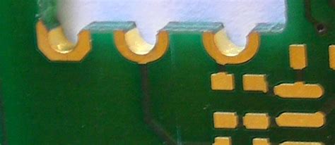
Tenting Vias
What is Via Tenting?
Via tenting is a process in which a via is covered with a thin layer of solder mask material on one or both sides of the PCB. This process helps to protect the via from environmental factors, such as moisture and dust, and prevents solder from flowing into the via during the soldering process.
Advantages of Via Tenting
- Protection: Tenting vias helps to protect the via from environmental factors, increasing the reliability and longevity of the PCB.
- Solder control: By covering the via with solder mask, tenting prevents solder from flowing into the via during the soldering process, reducing the risk of shorts and other defects.
- Improved insulation: The solder mask layer provides additional insulation, reducing the risk of electrical shorts between adjacent vias or traces.
- Enhanced aesthetics: Tenting vias can improve the overall appearance of the PCB by creating a more uniform surface finish.
Disadvantages of Via Tenting
- Increased cost: Tenting vias requires an additional manufacturing step, which can increase the overall cost of the PCB.
- Potential for air pockets: If not properly applied, the solder mask layer can trap air pockets around the via, leading to reliability issues.
- Reduced thermal conductivity: The solder mask layer can act as a thermal insulator, reducing the ability of the via to dissipate heat.
Applications of Via Tenting
Via tenting is commonly used in PCB designs that require:
- High reliability: In applications where the PCB will be exposed to harsh environments, such as automotive or aerospace systems, tenting vias can help to improve the overall reliability of the board.
- Solder mask defined pads: When using solder mask defined (SMD) pads, tenting vias can help to prevent solder from flowing into the via during the soldering process.
- High-density designs: In high-density PCB layouts, tenting vias can help to prevent shorts between adjacent vias or traces.

Plugged Vias
What are Plugged Vias?
Plugged vias are vias that are filled with a non-conductive material, such as epoxy or resin, to create a solid, planar surface on the PCB. This process helps to improve the structural integrity of the board and enables the placement of components or traces directly over the via.
Advantages of Plugged Vias
- Improved structural integrity: By filling the via with a solid material, plugged vias help to strengthen the PCB and reduce the risk of mechanical failure.
- Increased layout flexibility: Plugged vias allow components or traces to be placed directly over the via, enabling more compact and efficient PCB layouts.
- Enhanced thermal conductivity: When filled with a thermally conductive material, plugged vias can help to dissipate heat more effectively than tented vias.
- Improved impedance control: Plugged vias can help to maintain consistent impedance across the PCB, which is crucial for high-speed signal integrity.
Disadvantages of Plugged Vias
- Increased cost: Plugging vias requires additional manufacturing steps and materials, which can increase the overall cost of the PCB.
- Potential for voids: If not properly filled, plugged vias can contain voids or air pockets, which can lead to reliability issues.
- Limited rework options: Once a via is plugged, it can be difficult to rework or repair if needed.
Applications of Plugged Vias
Plugged vias are commonly used in PCB designs that require:
- High-density layouts: Plugged vias enable the placement of components or traces directly over the via, allowing for more compact and efficient PCB layouts.
- Controlled impedance: In high-speed designs, plugged vias can help to maintain consistent impedance across the PCB, improving signal integrity.
- Mechanical stability: In applications where the PCB will be subjected to mechanical stress, such as vibration or shock, plugged vias can help to improve the structural integrity of the board.

Via in Pad
What is Via in Pad?
Via in pad is a design technique in which a via is placed directly within a component pad, allowing for a more compact PCB layout. This technique is often used in high-density designs where space is limited, as it eliminates the need for a separate via pad and trace.
Advantages of Via in Pad
- Space savings: By placing the via directly within the component pad, via in pad allows for more compact PCB layouts, reducing the overall size of the board.
- Reduced inductance: Via in pad can help to reduce the inductance of the connection between the component and the via, improving signal integrity.
- Improved thermal conductivity: When used with a thermally conductive via fill material, via in pad can help to dissipate heat more effectively from the component to the PCB.
- Simplified assembly: Via in pad can simplify the assembly process by eliminating the need for a separate via pad and trace.
Disadvantages of Via in Pad
- Increased manufacturing complexity: Via in pad requires precise alignment between the component pad and the via, which can increase the complexity of the manufacturing process.
- Potential for solder wicking: If not properly designed, via in pad can lead to solder wicking into the via during the soldering process, causing defects or reliability issues.
- Limited component compatibility: Not all components are suitable for use with via in pad, as the technique requires a certain minimum pad size and spacing.
Applications of Via in Pad
Via in pad is commonly used in PCB designs that require:
- High-density layouts: Via in pad allows for more compact PCB layouts, making it well-suited for high-density designs where space is limited.
- High-speed signals: By reducing the inductance of the connection between the component and the via, via in pad can help to improve signal integrity in high-speed designs.
- Thermally sensitive components: When used with a thermally conductive via fill material, via in pad can help to dissipate heat more effectively from thermally sensitive components.

Comparing Tenting Vias, Plugged Vias, and Via in Pad
To better understand the differences between tenting vias, plugged vias, and via in pad, let’s compare them across several key factors:
| Factor | Tenting Vias | Plugged Vias | Via in Pad |
|---|---|---|---|
| Protection | Good | Excellent | Fair |
| Solder Control | Good | Excellent | Fair |
| Thermal Conductivity | Fair | Good | Excellent |
| Structural Integrity | Fair | Excellent | Good |
| Layout Flexibility | Fair | Good | Excellent |
| Manufacturing Cost | Moderate | High | Moderate |
| Manufacturing Complexity | Moderate | High | High |
As we can see from the table, each technique has its own strengths and weaknesses, and the choice of which to use will depend on the specific requirements of the PCB design.
Frequently Asked Questions (FAQ)
- What are the main differences between tenting vias, plugged vias, and via in pad?
Tenting vias are covered with a thin layer of solder mask material, plugged vias are filled with a non-conductive material, and via in pad involves placing a via directly within a component pad. Each technique offers different benefits and trade-offs in terms of protection, thermal conductivity, layout flexibility, and manufacturing complexity.
- When should I use tenting vias in my PCB design?
Tenting vias are best used in applications that require high reliability, solder mask defined pads, or high-density designs. They offer good protection against environmental factors and help to prevent solder from flowing into the via during the soldering process.
- What are the advantages of using plugged vias?
Plugged vias offer improved structural integrity, increased layout flexibility, enhanced thermal conductivity, and improved impedance control. They are well-suited for high-density layouts, controlled impedance designs, and applications that require mechanical stability.
- Are there any limitations to using via in pad?
Yes, via in pad requires precise alignment between the component pad and the via, which can increase manufacturing complexity. Additionally, not all components are suitable for use with via in pad, as the technique requires a certain minimum pad size and spacing.
- How do I choose between tenting vias, plugged vias, and via in pad for my PCB design?
The choice between tenting vias, plugged vias, and via in pad will depend on the specific requirements of your PCB design. Consider factors such as the level of protection needed, thermal conductivity requirements, layout density, manufacturing cost, and complexity. Consult with your PCB manufacturer to determine the best option for your specific application.
Conclusion
In conclusion, tenting vias, plugged vias, and via in pad are three important techniques used in PCB design to connect different layers of a multilayer board. Each technique offers its own unique benefits and trade-offs, and the choice of which to use will depend on the specific requirements of the PCB design.
Tenting vias offer good protection against environmental factors and help to prevent solder from flowing into the via during the soldering process. Plugged vias provide improved structural integrity, increased layout flexibility, and enhanced thermal conductivity. Via in pad allows for more compact PCB layouts and can help to reduce the inductance of the connection between the component and the via.
When choosing between these techniques, it is important to consider factors such as the level of protection needed, thermal conductivity requirements, layout density, manufacturing cost, and complexity. By understanding the strengths and weaknesses of each technique and consulting with your PCB manufacturer, you can select the best option for your specific application, ensuring a reliable and high-performance PCB design.
Leave a Reply