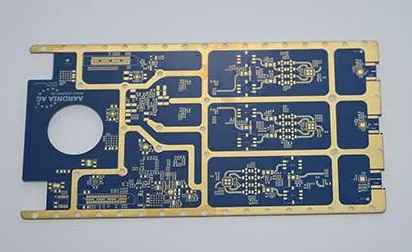
Introduction to RF PCB Boards
An RF (radio frequency) PCB (printed circuit board) is a special type of PCB designed to operate at radio frequencies. RF PCBs are used in products that transmit or receive radio signals such as cell phones, WiFi routers, Bluetooth devices, and radar systems. The RF circuitry on the PCBs converts signals into radio waves and vice versa.
Some key characteristics of RF PCBs:
- Designed for high frequency operation from 3 kHz to 300 GHz
- Controlled impedance traces for proper signal integrity
- Good dielectric materials with low loss tangent
- Proper grounding and shielding techniques
- Precision fabrication to avoid mismatches and reflections
RF PCB Design Considerations
Designing an RF PCB requires special considerations compared to a standard digital PCB:
Impedance Control
Maintaining a constant controlled impedance across traces is critical for RF signals. Any discontinuities or impedance mismatches can reflect signals and introduce loss and noise. Common impedance values are 50 or 75 ohms.
Layer Stackup
The layer stackup must be properly designed with reference planes and dielectric materials oriented to control impedance, reduce cross-talk, and limit signal losses. Common RF stackups use Rogers circuit materials.
Passive Components
Passive components like resistors, capacitors, and inductors need tight tolerances and appropriate packaging for RF functionality. Surface mount devices are preferred.
Shielding
Sensitive RF circuitry needs shielding from radiated emissions and external interference. Shielding cans, vias, or grounded copper polygons help isolate RF circuitry.
Antennas and Transitions
Integrated antennas, coaxial connectors, microstrip launches, and other electromechanical interfaces require special RF modeling and design expertise.
RF PCB Manufacturing and Testing

Manufacturing RF PCBs requires advanced fabrication processes:
- Fine line/space capabilities, 6-8 mil lines/spaces typical
- Tight impedance tolerances, within ±5%
- Smooth copper and low surface roughness
- Precise dielectric constant and thickness
- Excellent registration and accuracy
RF PCBs also require specialized testing:
- Time domain reflectometry to validate trace impedance
- Vector network analysis for insertion loss, return loss, VSWR
- Signal integrity analysis at frequency
- Radiated emissions testing
Working with an experienced PCB manufacturer with RF capabilities is highly recommended for a successful RF PCB build.
Conclusion
RF design requires specialized skills and processes in PCB layout, material selection, modeling, fabrication, assembly, and test. Attention to impedance control, transmission lines, shielding, and other RF considerations during design is mandatory. Partnering with experts in RF PCB design and manufacturing ensures your wireless and high frequency products function as intended.
Frequently Asked Questions
Q: What are some typical RF frequencies used in PCBs?
A: Common RF frequency ranges include:
- 3 kHz to 300 kHz for RFID, wireless charging
- 300 kHz to 3 MHz for AM radio
- 3 MHz to 300 MHz for FM radio, TV, WiFi, Bluetooth
- 300 MHz to 3 GHz for 4G/5G cellular, GPS, satellite communications
- 3 GHz to 30 GHz for 5G, radar, microwave radio
- 30 GHz to 300 GHz for millimeter wave 5G, satellite
Q: What materials are used for RF PCBs?
A: Common RF PCB substrate materials include:
- Rogers RO4003C, RO4350B for circuits up to 3 GHz
- Rogers RO4835, RO4000-6 for mmWave above 30 GHz
- Taconic RF-35, RF-60A for low loss circuits
- Isola Astra MT77 for low cost RF designs
- PTFE composites for maximum performance
Q: How are RF PCBs tested during manufacturing?
A: Typical RF PCB tests include:
- Time domain reflectometry (TDR) to validate trace impedance
- Vector network analysis (VNA) for S-parameters, insertion loss
- Power integrity analysis at frequency
- VSWR for impedance matching
- Radiated emissions testing for unintended emissions
- Functional RF signal testing for wireless specs
Q: What are some best practices for RF layout?
A: Best practices for RF PCB layout include:
- Maintain constant controlled impedance for all traces
- Use adequate stitching vias around traces as RF return paths
- Keep out flooded copper planes under traces to avoid attenuation
- Route traces orthogonally to avoid coupling and crosstalk
- Provide proper RF component pads, annular rings, and thermal relief
- Add parasitic extraction in layout tools to model RF performance
Q: How can EMI be minimized in an RF design?
A: Recommendations for minimizing EMI in RF designs:
- Use shielding cans over sensitive RF components
- Place ground vias around the perimeter of the PCB
- Include Pi filters on signal cables entering/exiting the enclosure
- Use ground and power planes in layer stackup
- Select RF components with low radiation profiles
- Model and measure far-field radiation during design
- Follow proper RF layout techniques for trace routing
Leave a Reply