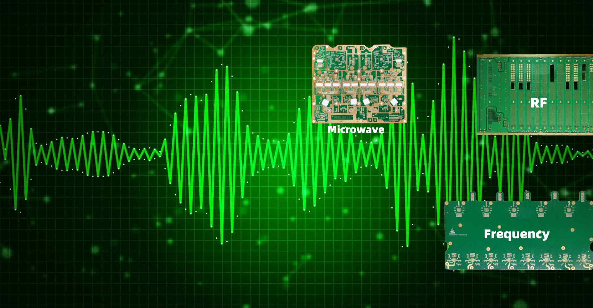
What are RF PCBs?
RF PCBs (radio frequency printed circuit boards) are circuit boards designed to operate at high frequencies from 3 kHz to 300 GHz. They are used in products like cell phones, Wi-Fi routers, Bluetooth devices, and other wireless electronics. RF PCBs differ from standard PCBs in their materials, layout, and fabrication.
RF PCB Materials
RF PCBs require specialized substrate materials to accommodate high frequency signals. Common materials include:
- FR-4 – Most affordable, suitable for lower RF frequencies
- PTFE/Teflon – Low loss, good performance above 3 GHz
- Ceramic-filled PTFE – Improved dielectric properties over FR-4
- Rogers – High performance and consistency, but costly
- LCP – Extremely low loss for mmWave applications
RF PCB Design Guidelines

Proper RF PCB design is critical for good signal integrity. Here are some key guidelines:
Impedance Control
Maintain controlled impedance across traces through consistent trace geometry and spacing. This prevents reflections and signal loss.
Stackup Design
Use thin dielectrics and plan layer stackup for short and direct routing. Minimize layer changes.
Bypass and Decoupling
Use capacitors and ground vias for bypassing and decoupling to suppress noise and transients.
Short Traces
Keep traces short. Maximum 1/20 wavelength of highest operating frequency. Use miters for corners.
Ground Plane and Returns
Use solid ground planes below signal layers for return paths. Improve isolation with guard traces.
Component Placement
Place components for shortest possible connections. Ground sensitive ICs directly to ground plane.
Vias
Minimize via counts. Use backdrilling for unused portions.
Comparison of PCB Materials for RF
| Material | Dielectric Constant | Loss Tangent | Frequency Range |
|---|---|---|---|
| FR-4 | 4.2-4.8 | 0.02 | < 3 GHz |
| PTFE | 2.1-2.2 | 0.001 | > 3 GHz |
| Ceramic PTFE | 3-10 | 0.003-0.004 | > 10 GHz |
| Rogers RO4350B | 3.48 | 0.0037 | > 5 GHz |
| LCP | 3 | 0.002 | mmWave (>30 GHz) |
FAQ
What are some challenges with RF PCB design?
Some key challenges are maintaining impedance control, minimizing reflections, accounting for skin effect losses, and handling higher temperatures from RF heating. Careful planning and simulation is necessary to achieve proper performance.
How are RF PCBs different from digital PCBs?
RF PCBs require much more attention to controlled impedance traces, stackup, layer changes, ground planes, and passive components to maintain signal integrity at high frequencies. They are also more prone to interference.
What fabrication considerations are there for RF PCBs?
RF PCB fabrication must be done with tight tolerances on trace width, dielectric thickness, and registration. High frequency boards may require advanced processes like laser drilling and stacked vias. Many boards also use immersion silver plating.
How are components laid out on a RF PCB?
Components are carefully placed to minimize trace lengths. Sensitive components are placed over a ground plane or shielding. Grouping of like components and circuit blocks improves isolation. Heat-generating components need thermal vias.
What types of connectors do RF PCBs use?
Common RF connectors include SMA, SSMA, SMP, and 2.92mm connectors. They maintain 50 ohm impedance and are rated up to at least 6GHz. High frequency boards may use 1.85mm or smaller micro coaxial connectors.

Leave a Reply