Tips for Creating High-Performance PCBs
Radio frequency (RF) circuit design requires careful attention to layout and routing to ensure signal integrity and minimize interference and losses. Here are some best practices to follow when designing RF boards:
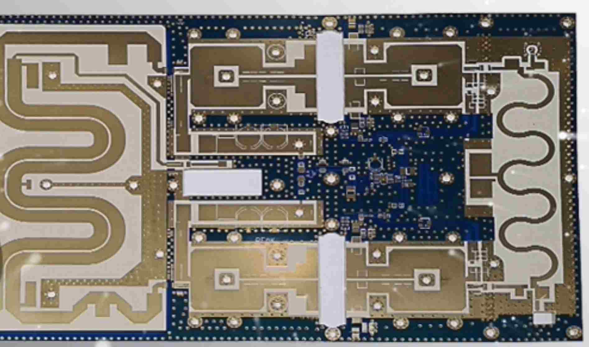
Use Proper Stackup
Selecting the right laminate and stackup is critical for RF boards. Some key considerations:
- Use high-frequency dielectric materials like Rogers or Arlon with tight dielectric constant (Dk) tolerances
- Minimize the number of laminate layers
- Include a grounded layer to isolate RF signals
- Place a solid ground plane next to RF layer to provide return paths
| Layer | Function |
|---|---|
| 1 | RF Signal |
| 2 | Ground Plane |
| 3 | DC Power |
| 4 | Ground Plane |
Follow Layout Guidelines
- Keep RF traces short and direct
- Avoid 90° angles – use arched or 45° trace corners
- Route RF traces over solid ground areas
- Isolate analog and digital sections
- Use stitching vias to connect ground layers
- Include shielding for sensitive traces
Minimize Passives
- Specify chip resistors and capacitors with tight tolerances
- Use smallest size 0201 or 01005 components
- Minimize lead lengths
- Keep passives close to ICs they support
Careful Component Placement
- Position ICs that need to interconnect close together
- Orient components to optimize routing
- Group like signals together
- Keep high-speed traces away from connectors or EMI sources
Validate with Simulation
- Use 3D EM simulation to model effects of routing
- Verify impedance matching and coupling
- Tune layout to meet RF performance targets
Following these guidelines will help ensure your RF PCB layout achieves the required signal performance. Evaluate stackup, routing, and placement thoroughly before finalizing design.
Frequently Asked Questions

What are some key RF design considerations?
Some key considerations for RF design include:
- Minimizing trace length and using proper impedance matching
- Selecting the right PCB materials and stackup
- Isolating analog and digital sections
- Following layout guidelines for trace widths, spacing, and angles
- Using proper grounding and shielding techniques
- Minimizing parasitics through component selection and placement
- Validating the design with EM and signal integrity simulations
How can I reduce interference on RF boards?
Strategies to reduce interference include:
- Use a solid ground plane to provide a low impedance return path
- Carefully route signals to avoid coupling between traces
- Space traces further apart or at right angles
- Use grounded coplanar waveguides or guard traces
- Include shielding cans over critical ICs
- Filter supply lines and I/O interfaces
What should I consider for material selection?
For RF boards, choose materials like Rogers or Arlon laminates that have consistent dielectric properties. Key considerations include:
- Dielectric constant and loss tangent
- Dielectric constant tolerance
- Glass transition temperature
- Coefficient of thermal expansion
- High frequency characteristics
- Availability of prepregs and cores in different thicknesses
How can I model RF performance prior to PCB fabrication?
3D EM simulation using tools like Ansys HFSS or Keysight ADS can extract S-parameters to model RF signal performance. These simulations can help identify and correct issues with:
- Impedance discontinuities
- Resonances
- Coupling between traces
- Signal losses
- Crosstalk
- Radiation effects
What are common stackup configurations for RF designs?
Common stackup configurations include:
- 4-layer with RF layer over ground plane
- 6-layer with RF layer between ground planes
- Stripline with RF traces sandwiched between two ground layers
- Microstrip with RF layer next to exposed plane
- Buried microstrip with RF layer buried between dielectric
The key is to have at least one uninterrupted ground plane next to the RF layer to provide a controlled impedance environment. Additional ground planes help shield signals.
Leave a Reply