Introduction to PCB Assembly
Printed Circuit Board (PCB) assembly is the process of attaching electronic components to a printed circuit board to create a functional electronic device. The process involves several steps, including PCB design, component selection, placement, soldering, and testing. In this article, we will provide a comprehensive overview of the PCB assembly process, including the materials and equipment used, the different assembly techniques, and the quality control measures employed to ensure the reliability and performance of the finished product.
What is a Printed Circuit Board?
A printed circuit board is a thin board made of fiberglass or other insulating material, with conductive tracks etched onto its surface. These tracks are used to connect electronic components, such as resistors, capacitors, and integrated circuits, to create a complete electronic circuit. PCBs are used in almost all electronic devices, from smartphones and laptops to industrial control systems and medical equipment.
Why is PCB Assembly Important?
PCB assembly is a critical process in the manufacturing of electronic devices. It determines the reliability, performance, and cost of the finished product. A well-designed and properly assembled PCB can ensure that the device functions as intended, while a poorly assembled PCB can lead to malfunctions, short circuits, and even safety hazards. Therefore, it is essential to follow best practices and quality control measures throughout the PCB assembly process.
PCB Assembly Materials and Equipment
PCB Materials
The most common material used for PCBs is FR-4, a type of fiberglass reinforced epoxy laminate. FR-4 is known for its high strength, good insulation properties, and resistance to heat and moisture. Other materials used for PCBs include:
- Polyimide: Used for high-temperature applications
- Teflon: Used for high-frequency applications
- Aluminum: Used for heat dissipation
- Flexible PCBs: Made of flexible plastic materials
Electronic Components
Electronic components are the building blocks of a PCB. They include:
- Resistors: Used to control current flow
- Capacitors: Used to store electrical charge
- Inductors: Used to store energy in a magnetic field
- Diodes: Used to allow current flow in one direction only
- Transistors: Used to amplify or switch electronic signals
- Integrated Circuits (ICs): Complex circuits packaged in a single chip
Soldering Equipment
Soldering is the process of joining electronic components to the PCB using a metal alloy called solder. The most common soldering techniques used in PCB assembly are:
- Wave Soldering: A automated process where the PCB is passed over a wave of molten solder
- Reflow Soldering: A process where solder paste is applied to the PCB, components are placed, and the board is heated to melt the solder
- Hand Soldering: A manual process where a soldering iron is used to apply solder to individual components
Inspection Equipment
Inspection is a critical step in the PCB assembly process to ensure the quality and reliability of the finished product. Common inspection equipment includes:
- Automated Optical Inspection (AOI): Uses cameras and image processing software to detect defects
- X-Ray Inspection: Uses X-rays to detect defects in solder joints and hidden components
- In-Circuit Testing (ICT): Uses probes to test the functionality of individual components and circuits

PCB Assembly Techniques
Through-Hole Assembly
Through-hole assembly is a traditional PCB assembly technique where component leads are inserted through holes drilled in the PCB and soldered to pads on the opposite side. This technique is used for larger components and provides a strong mechanical connection. However, it is slower and more labor-intensive than surface mount assembly.
Surface Mount Assembly
Surface mount assembly is a more modern PCB assembly technique where components are mounted directly onto pads on the surface of the PCB. This technique allows for smaller components and higher component density, resulting in smaller and more complex PCBs. Surface mount assembly is typically done using reflow soldering, where solder paste is applied to the pads, components are placed, and the board is heated to melt the solder.
Mixed Assembly
Mixed assembly is a combination of through-hole and surface mount assembly techniques. This is often used when a PCB requires both large through-hole components and small surface mount components. Mixed assembly can be more complex and time-consuming than either technique alone, but it offers greater flexibility in PCB design.

PCB Assembly Process
PCB Design
The first step in the PCB assembly process is PCB design. This involves creating a schematic diagram of the electronic circuit and a layout of the PCB. The schematic diagram shows how the components are connected electrically, while the layout shows the physical placement of the components on the PCB. PCB design software is used to create these files, which are then sent to a PCB manufacturer for fabrication.
Component Selection and Procurement
Once the PCB design is complete, the next step is to select and procure the electronic components. This involves choosing components that meet the electrical and mechanical requirements of the circuit, as well as considering factors such as cost, availability, and lead time. Components are typically sourced from distributors or directly from manufacturers.
PCB Fabrication
PCB fabrication is the process of manufacturing the bare PCB based on the design files. This typically involves the following steps:
- Printing the circuit pattern onto a photosensitive film
- Exposing the film onto a copper-clad board
- Developing the exposed areas to remove the unwanted copper
- Etching away the remaining copper to create the circuit traces
- Drilling holes for through-hole components
- Applying a protective solder mask and silkscreen layer
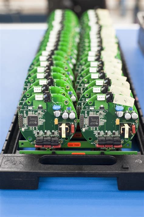
Component Placement
Once the bare PCB is fabricated, the next step is to place the components onto the board. This is typically done using automated pick-and-place machines, which use vacuum nozzles to pick up components from reels or trays and place them onto the PCB with high precision. The placement program is generated from the PCB layout file and tells the machine where to place each component.
Soldering
After the components are placed, the PCB is sent to the soldering station. For surface mount assembly, solder paste is applied to the pads using a stencil or syringe, and the board is heated in a reflow oven to melt the solder and form a permanent connection. For through-hole assembly, the leads are inserted through the holes and soldered using a wave soldering machine or by hand.
Inspection and Testing
After soldering, the PCB undergoes a series of inspections and tests to ensure that it is functioning properly and meets the required specifications. This may include:
- Visual inspection for defects such as solder bridges, cold solder joints, or misaligned components
- Automated optical inspection (AOI) using cameras and image processing software
- X-ray inspection to check for hidden defects or voids in solder joints
- In-circuit testing (ICT) to verify the functionality of individual components and circuits
- Functional testing to ensure that the complete assembly performs as intended
Rework and Repair
If defects are found during inspection and testing, the PCB may need to be reworked or repaired. This involves removing the defective component, cleaning the site, and replacing it with a new component. Rework can be done by hand or using specialized equipment, depending on the type and location of the defect.

Quality Control in PCB Assembly
Quality control is a critical aspect of PCB assembly to ensure the reliability and performance of the finished product. Some of the key quality control measures include:
Process Control
Process control involves monitoring and controlling the various steps in the PCB assembly process to ensure consistency and minimize defects. This may include:
- Controlling the temperature and humidity of the assembly environment
- Calibrating and maintaining equipment to ensure proper operation
- Using statistical process control (SPC) techniques to monitor process variables and identify trends or anomalies
Traceability
Traceability involves maintaining records of the materials, equipment, and processes used in the assembly of each PCB. This allows for quick identification and resolution of issues if defects are found later in the process or in the field. Traceability typically involves using barcodes or RFID tags to track individual PCBs and components throughout the assembly process.
ESD Control
Electrostatic discharge (ESD) can damage sensitive electronic components and cause latent defects that may not be detected during testing. ESD control measures are used to prevent static buildup and discharge, such as:
- Using grounded work surfaces and wrist straps for operators
- Storing components in ESD-safe packaging
- Using ionizers to neutralize static charges in the assembly environment
Conformal Coating
Conformal coating is a protective layer applied to the PCB after assembly to protect it from moisture, dust, and other environmental factors. Conformal coating can be applied by spraying, dipping, or brushing, and can be made of various materials such as acrylic, silicone, or polyurethane.
PCB Assembly Challenges and Trends
Miniaturization
As electronic devices become smaller and more complex, PCBs must also become smaller and more densely packed with components. This presents challenges for PCB assembly, such as:
- Handling and placing tiny components accurately
- Ensuring adequate soldering and inspection of fine-pitch components
- Managing heat dissipation in high-density designs
High-Speed and High-Frequency Designs
PCBs for high-speed and high-frequency applications, such as 5G wireless and automotive radar, require careful design and assembly to ensure signal integrity and minimize electromagnetic interference (EMI). Challenges include:
- Controlling impedance and minimizing signal reflections
- Managing crosstalk and EMI
- Ensuring proper grounding and shielding
Flexible and Stretchable PCBs
Flexible and stretchable PCBs are becoming increasingly common in wearable electronics, medical devices, and other applications where conformability and durability are important. Challenges include:
- Handling and assembling thin, flexible materials
- Ensuring reliable connections and strain relief
- Testing and inspecting for defects in non-planar designs
Sustainable and Eco-Friendly Materials
As environmental concerns grow, there is increasing demand for sustainable and eco-friendly PCB materials and assembly processes. This includes:
- Using halogen-free and lead-free materials
- Minimizing waste and energy consumption in the assembly process
- Designing for recyclability and end-of-life management
FAQs
What is the difference between through-hole and surface mount assembly?
Through-hole assembly involves inserting component leads through holes in the PCB and soldering them to pads on the opposite side, while surface mount assembly involves placing components directly onto pads on the surface of the PCB. Surface mount assembly allows for smaller components and higher density, while through-hole assembly provides stronger mechanical connections.
What is solder paste and how is it used in PCB assembly?
Solder paste is a mixture of tiny solder particles suspended in a flux medium. It is applied to the pads on a PCB using a stencil or syringe, and then the components are placed onto the paste. When the board is heated in a reflow oven, the solder particles melt and form a permanent connection between the component leads and the pads.
What is the purpose of a solder mask on a PCB?
A solder mask is a protective layer applied to the PCB that covers the copper traces and leaves only the pads and other areas that need to be soldered exposed. The solder mask prevents solder from bridging between traces and protects the board from moisture and other contaminants.
What is the difference between a single-sided and a double-sided PCB?
A single-sided PCB has components and traces on only one side of the board, while a double-sided PCB has components and traces on both sides. Double-sided PCBs allow for higher component density and more complex designs, but they are also more expensive and challenging to assemble than single-sided PCBs.
What are some common defects that can occur during PCB assembly?
Some common defects that can occur during PCB assembly include:
- Solder bridges: Unintended connections between adjacent pads or traces
- Cold solder joints: Weak or incomplete solder connections due to insufficient heat or poor wetting
- Component misalignment: Components placed inaccurately or rotated on the pads
- Tombstoning: One end of a component lifting off the pad due to uneven heating or surface tension
- Insufficient or excessive solder: Too little or too much solder on the pads, leading to weak or bulky connections
Conclusion
PCB assembly is a complex and critical process in the manufacturing of electronic devices. It involves a range of materials, equipment, and techniques, and requires careful design, process control, and quality assurance to ensure the reliability and performance of the finished product. As electronic devices continue to evolve and become more sophisticated, PCB assembly faces new challenges and opportunities in areas such as miniaturization, high-speed design, flexible and stretchable materials, and sustainability. By staying up-to-date with the latest technologies and best practices, PCB assemblers can meet these challenges and deliver high-quality, innovative products to their customers.
Leave a Reply