Understanding the Different Types of PCB Vias
Printed Circuit Boards (PCBs) are essential components in modern electronic devices, connecting various components and enabling the flow of electrical signals. One crucial aspect of PCB design is the use of vias, which are conductive pathways that allow signals to pass through different layers of the board. In this comprehensive article, we will explore the different types of PCB vias, their characteristics, and their applications.
What are PCB Vias?
PCB vias are small holes drilled through the layers of a printed circuit board, which are then plated with a conductive material, typically copper. These conductive pathways enable electrical signals to travel between different layers of the PCB, allowing for more complex and compact designs. Vias play a critical role in PCB layout and are essential for creating efficient and reliable electronic devices.
The Importance of PCB Vias
PCB vias serve several important functions in the design and manufacturing of printed circuit boards:
- Interconnectivity: Vias allow electrical signals to pass through different layers of the PCB, enabling the connection of components on different sides of the board or in different layers.
- Space Optimization: By utilizing vias, designers can create more compact PCB layouts, as components can be placed on different layers and connected through vias, rather than requiring larger traces on a single layer.
- Signal Integrity: Vias help maintain signal integrity by providing a direct path for signals to travel between layers, minimizing the distance traveled and reducing the potential for signal degradation.
- Heat Dissipation: Thermal vias, a specific type of via, can be used to dissipate heat from components, helping to prevent overheating and ensure the longevity of the device.
Types of PCB Vias
There are several types of PCB vias, each with its own characteristics and applications. The most common types of vias include:
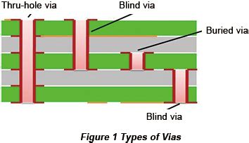
1. Through Hole Vias
Through hole vias are the most basic and widely used type of via in PCB design. These vias are drilled completely through all layers of the PCB and are plated with a conductive material, creating an electrical connection between the layers. Through hole vias are typically used for connecting components to the board, such as connectors, switches, and large components like capacitors and resistors.
Advantages of Through Hole Vias
- Strong mechanical connection
- Easy to solder and inspect
- Suitable for high-power applications
- Compatible with through-hole components
Disadvantages of Through Hole Vias
- Require more space on the PCB
- Limit the routing of traces on inner layers
- More expensive to manufacture compared to other via types
2. Blind Vias
Blind vias are a type of via that starts on an outer layer of the PCB and terminates on an inner layer, without passing through the entire board. These vias are typically used to connect an outer layer to an inner layer, allowing for more compact designs and improved signal integrity.
Advantages of Blind Vias
- Reduce the overall size of the PCB
- Improve signal integrity by reducing the via length
- Allow for more flexibility in component placement
- Enable higher density designs
Disadvantages of Blind Vias
- More expensive to manufacture compared to through hole vias
- Require specialized manufacturing processes
- Limited to connecting outer layers to inner layers
3. Buried Vias
Buried vias are similar to blind vias but are located entirely within the inner layers of the PCB. These vias connect two or more inner layers without being visible on the outer layers of the board. Buried vias are used to create complex interconnections between inner layers, allowing for even more compact and dense PCB designs.
Advantages of Buried Vias
- Enable high-density designs
- Improve signal integrity by reducing the via length
- Allow for more flexibility in routing traces on inner layers
- Reduce the overall size of the PCB
Disadvantages of Buried Vias
- Most expensive to manufacture among via types
- Require specialized manufacturing processes
- Limited to connecting inner layers only
- Difficult to inspect and troubleshoot
4. Microvia
Microvias are small, high-density vias that are typically less than 150 microns in diameter. These vias are used in advanced PCB designs, particularly in high-frequency and high-speed applications. Microvias are usually laser-drilled and can be stacked or staggered to create complex interconnections between layers.
Advantages of Microvias
- Enable ultra-high-density designs
- Improve signal integrity by minimizing via length and inductance
- Allow for more compact and efficient PCB layouts
- Suitable for high-frequency and high-speed applications
Disadvantages of Microvias
- Require specialized manufacturing processes and equipment
- More expensive to manufacture compared to larger via types
- Limited to connecting a few layers, typically up to four layers
5. Thermal Vias
Thermal vias are designed to dissipate heat from components on the PCB, helping to prevent overheating and ensure the longevity of the device. These vias are typically placed under or near heat-generating components, such as power transistors or voltage regulators, and are connected to a large copper area or a dedicated thermal pad on the board.
Advantages of Thermal Vias
- Help dissipate heat from components
- Improve the overall thermal performance of the PCB
- Increase the lifespan of heat-generating components
- Allow for more compact designs by reducing the need for external heatsinks
Disadvantages of Thermal Vias
- Require additional space on the PCB
- May increase the overall manufacturing cost
- Can affect the routing of traces on inner layers

Choosing the Right Type of PCB Via
When selecting the appropriate type of via for your PCB design, consider the following factors:
- PCB Complexity: The complexity of your PCB design will determine the types of vias required. Simple designs may only require through hole vias, while more complex designs may benefit from blind, buried, or microvias.
- Signal Integrity: Consider the signal integrity requirements of your design. High-speed and high-frequency applications may require microvias or blind vias to minimize via length and inductance.
- Manufacturing Cost: The cost of manufacturing increases with the complexity of the via structure. Through hole vias are the most cost-effective, while buried vias and microvias are more expensive.
- Component Placement: The placement of components on the PCB will influence the choice of via type. Through hole vias are suitable for connecting through-hole components, while blind and buried vias offer more flexibility in component placement.
- Thermal Management: If your design includes heat-generating components, consider incorporating thermal vias to improve heat dissipation and overall thermal performance.

PCB Via Manufacturing Processes
The manufacturing process for PCB vias varies depending on the type of via and the complexity of the design. The most common manufacturing processes include:
1. Mechanical Drilling
Mechanical drilling is the most common method for creating through hole vias. A drill bit is used to create holes through all layers of the PCB, which are then plated with a conductive material. This process is suitable for larger via sizes and is relatively cost-effective.
2. Laser Drilling
Laser drilling is used to create smaller vias, such as microvias. A focused laser beam is used to create holes in the PCB layers, which are then plated with a conductive material. This process allows for the creation of high-density vias and is suitable for advanced PCB designs.
3. Sequential Lamination
Sequential lamination is a process used to create blind and buried vias. The PCB layers are laminated and drilled in stages, allowing for the creation of vias that start or stop at specific layers. This process is more complex and expensive than mechanical drilling but enables more advanced PCB designs.

Best Practices for PCB Via Design
To ensure optimal performance and manufacturability of your PCB, consider the following best practices when designing vias:
- Via Size: Choose an appropriate via size based on the current requirements and the available space on the PCB. Larger vias can handle higher currents but occupy more space, while smaller vias enable higher density designs but have lower current carrying capacity.
- Via Spacing: Maintain sufficient spacing between vias and other components to ensure proper manufacturability and signal integrity. Consult with your PCB manufacturer for recommended via spacing guidelines.
- Aspect Ratio: The aspect ratio of a via refers to the ratio of its depth to its diameter. Maintain an appropriate aspect ratio to ensure reliable plating and avoid manufacturing issues. A typical aspect ratio for through hole vias is 8:1, while microvias may have aspect ratios up to 1:1.
- Via Stacking: When using microvias, consider stacking them to create connections between multiple layers. Stacked microvias can enable higher density designs and improve signal integrity.
- Thermal Management: Incorporate thermal vias in your design to dissipate heat from components effectively. Place thermal vias under or near heat-generating components and connect them to a large copper area or a dedicated thermal pad.
Frequently Asked Questions (FAQ)
1. What is the difference between a blind via and a buried via?
A blind via starts on an outer layer and terminates on an inner layer, while a buried via is located entirely within the inner layers of the PCB. Blind vias are used to connect outer layers to inner layers, while buried vias connect two or more inner layers without being visible on the outer layers.
2. Can microvias be used in high-power applications?
Microvias are typically used in high-frequency and high-speed applications, where signal integrity is crucial. Due to their small size, microvias have limited current carrying capacity and are not suitable for high-power applications. Through hole vias or larger blind/buried vias are more appropriate for high-power applications.
3. How do I determine the appropriate via size for my PCB design?
The appropriate via size depends on several factors, including the current requirements, available space on the PCB, and the manufacturing capabilities of your PCB supplier. Consult with your PCB manufacturer for recommended via sizes based on your specific design requirements.
4. Are there any limitations on the number of layers that can be connected using vias?
The number of layers that can be connected using vias depends on the type of via and the manufacturing capabilities of your PCB supplier. Through hole vias can connect all layers of the PCB, while blind and buried vias are limited to connecting outer layers to inner layers or connecting inner layers only. Microvias are typically limited to connecting a few layers, usually up to four layers.
5. How do thermal vias help with heat dissipation in PCB designs?
Thermal vias are designed to transfer heat from heat-generating components to a large copper area or a dedicated thermal pad on the PCB. By providing a low-resistance path for heat to dissipate, thermal vias help to prevent overheating and ensure the longevity of the components and the overall device. Thermal vias are typically placed under or near heat-generating components, such as power transistors or voltage regulators.
Conclusion
PCB vias are essential components in modern electronic devices, enabling the interconnection of layers and components on printed circuit boards. Understanding the different types of vias, their characteristics, and their applications is crucial for designing efficient, reliable, and high-performance PCBs.
Through hole vias, blind vias, buried vias, microvias, and thermal vias each have their own advantages and disadvantages, and the choice of via type depends on factors such as PCB complexity, signal integrity requirements, manufacturing cost, component placement, and thermal management needs.
By following best practices for via design and working closely with experienced PCB manufacturers, designers can create advanced and reliable PCBs that meet the ever-increasing demands of modern electronic devices.
As technology continues to advance, the importance of PCB vias in enabling compact, high-performance, and cost-effective electronic devices will only continue to grow. By staying informed about the latest developments in via technology and design techniques, PCB designers can create innovative solutions that push the boundaries of what is possible in the world of electronics.
| Via Type | Description | Advantages | Disadvantages |
|---|---|---|---|
| Through Hole Via | Drilled through all layers and plated with conductive material | Strong mechanical connection, easy to solder and inspect, suitable for high-power applications | Require more space, limit trace routing on inner layers, more expensive |
| Blind Via | Starts on an outer layer and terminates on an inner layer | Reduce PCB size, improve signal integrity, allow flexible component placement | More expensive, require specialized manufacturing, limited to outer-inner connections |
| Buried Via | Located entirely within inner layers, connecting two or more inner layers | Enable high-density designs, improve signal integrity, allow flexible trace routing | Most expensive, require specialized manufacturing, difficult to inspect |
| Microvia | Small, high-density vias (typically <150 microns in diameter), used in advanced PCB designs | Enable ultra-high-density designs, improve signal integrity, suitable for high-speed | Require specialized manufacturing and equipment, limited to connecting few layers |
| Thermal Via | Designed to dissipate heat from components, connected to large copper area or dedicated thermal pad | Help dissipate heat, improve thermal performance, increase component lifespan | Require additional space, may increase manufacturing cost, can affect trace routing |
Leave a Reply