What is Impedance Matching in PCB Design?
Impedance matching is a critical aspect of PCB design that ensures optimal signal integrity and power transfer between a source and load. In PCB design, impedance matching refers to the process of matching the characteristic impedance of a transmission line (such as a PCB trace) to the impedance of the source and load connected to it. This is done to minimize signal reflections, reduce power loss, and improve overall system performance.
When a signal travels along a transmission line, it encounters a characteristic impedance (Z0) determined by the physical properties of the line, such as its width, thickness, and the dielectric constant of the surrounding material. If the impedance of the source and load matches the characteristic impedance of the transmission line, the signal can propagate without reflections, resulting in optimal power transfer and signal integrity.
Importance of Impedance Matching
Impedance matching is essential in high-speed PCB design for several reasons:
-
Signal Integrity: Proper impedance matching minimizes signal reflections, which can cause distortion, ringing, and other signal integrity issues. These problems can lead to data corruption, reduced system performance, and even device failure.
-
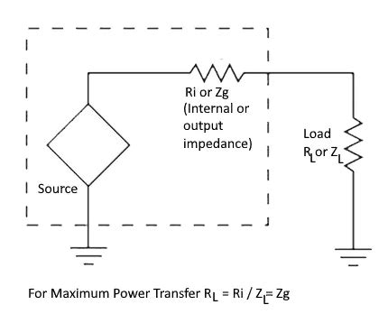
Power Transfer: When the impedance of the source, transmission line, and load are matched, maximum power transfer occurs. This is particularly important in applications where power efficiency is critical, such as in battery-powered devices or high-power systems.
-
EMI Reduction: Impedance mismatches can cause signal reflections that lead to increased electromagnetic interference (EMI). By ensuring proper impedance matching, designers can minimize EMI and improve the overall electromagnetic compatibility (EMC) of the system.
-
Reliable Communication: In high-speed communication systems, such as USB, HDMI, or Ethernet, impedance matching is crucial for ensuring reliable data transmission. Mismatches can cause signal degradation, leading to reduced data rates and potential communication failures.
Impedance Matching Techniques
There are several techniques used to achieve impedance matching in PCB design, including:
Resistive Matching
Resistive matching involves adding series or parallel resistors to the transmission line to match the impedance of the source and load. This method is simple and effective but can result in power loss due to the added resistance. Resistive matching is often used in low-frequency applications or when power loss is not a primary concern.
Reactive Matching
Reactive matching uses inductors and capacitors to match the impedance without introducing resistive losses. This method is more complex than resistive matching but offers better power efficiency. Reactive matching is commonly used in high-frequency applications, such as RF and microwave circuits.
Transformer Matching
Transformer matching uses a transformer to match the impedance between the source and load. This method provides galvanic isolation and can be used to match impedances with different voltage levels. Transformer matching is often used in power electronics and audio applications.
Stub Matching
Stub matching involves adding a short or open-circuited transmission line (stub) to the main transmission line to cancel out the reactive part of the impedance. This method is widely used in RF and microwave circuits, where the wavelength of the signal is comparable to the size of the PCB traces.

PCB Design Considerations for Impedance Matching
To achieve effective impedance matching in PCB design, several factors must be considered:
Trace Width and Thickness
The width and thickness of PCB traces directly affect their characteristic impedance. Wider traces have lower impedance, while thinner traces have higher impedance. To achieve a specific target impedance, designers must carefully calculate and control the trace dimensions.
Dielectric Constant
The dielectric constant (εr) of the PCB material influences the characteristic impedance of the traces. Materials with higher dielectric constants result in lower impedance traces, while those with lower dielectric constants yield higher impedance traces. Common PCB materials, such as FR-4, have a dielectric constant of around 4.2, but high-frequency laminates with lower dielectric constants are available for more demanding applications.
Trace Spacing
The spacing between PCB traces can impact their impedance and crosstalk. Closely spaced traces have higher mutual capacitance, which can lower their impedance and increase crosstalk. To maintain the target impedance and minimize crosstalk, designers must adhere to minimum spacing rules and use appropriate shielding techniques when necessary.
Via Design
Vias are an essential part of multi-layer PCB design but can introduce impedance discontinuities if not designed properly. To minimize the impact of vias on impedance, designers can use techniques such as via stitching, back-drilling, or buried vias. These methods help to reduce the capacitance and inductance associated with vias, thereby maintaining the target impedance.
Termination
Proper termination is crucial for impedance matching and signal integrity. Termination techniques, such as series termination, parallel termination, or AC termination, help to absorb signal reflections and prevent ringing. The choice of termination depends on factors such as the signal frequency, trace length, and the characteristics of the source and load.

Zero Resistance Impedance Matching
Zero resistance impedance matching is a special case where the source and load impedances are matched to the characteristic impedance of the transmission line without using any additional resistive elements. This method offers the advantage of minimizing power loss while maintaining optimal signal integrity.
To achieve zero resistance impedance matching, designers must carefully control the PCB layout and layer stackup. Some key considerations include:
-
Microstrip vs. Stripline: Microstrip and stripline are two common transmission line structures used in PCB design. Microstrip traces are routed on the outer layers of the PCB, while stripline traces are embedded within the inner layers. Each structure has its own characteristic impedance and design rules, which must be followed to achieve zero resistance matching.
-
Differential Pairs: Differential signaling is widely used in high-speed communication interfaces, such as USB, HDMI, and PCIe. To achieve zero resistance matching for differential pairs, designers must ensure that the traces have equal length, maintain a consistent spacing, and follow the appropriate routing guidelines.
-
Ground Planes: Proper grounding is essential for zero resistance impedance matching. Designers must provide adequate ground planes and ensure that the return path for the signals is well-defined. This helps to minimize inductance and maintain the target impedance.
-
Simulation and Modeling: To achieve zero resistance impedance matching, designers often use simulation tools and mathematical models to predict the behavior of the transmission lines. These tools help to optimize the PCB layout and layer stackup, ensuring that the target impedance is achieved without the need for additional resistive elements.

Impedance Matching Examples
To illustrate the importance of impedance matching, consider the following examples:
Example 1: Unmatched Transmission Line
Suppose a 50Ω source is connected to a 75Ω load through a 50Ω transmission line. In this case, the impedance of the load does not match the characteristic impedance of the transmission line, resulting in signal reflections and power loss.
The reflection coefficient (Γ) can be calculated using the following formula:
Γ = (ZL – Z0) / (ZL + Z0)
Where:
– ZL is the load impedance (75Ω)
– Z0 is the characteristic impedance of the transmission line (50Ω)
Plugging in the values, we get:
Γ = (75 – 50) / (75 + 50) = 0.2
This means that 20% of the incident power is reflected back to the source, while only 80% is delivered to the load. The power loss and signal reflections can cause signal integrity issues and degrade system performance.
Example 2: Matched Transmission Line
Now, consider the same 50Ω source connected to a 50Ω load through a 50Ω transmission line. In this case, the impedance of the source, transmission line, and load are perfectly matched.
Using the same formula as before, we get:
Γ = (50 – 50) / (50 + 50) = 0
A reflection coefficient of zero indicates that there are no signal reflections, and 100% of the power is delivered to the load. This example demonstrates the importance of impedance matching in ensuring optimal signal integrity and power transfer.
FAQ
1. What is the difference between characteristic impedance and input impedance?
Characteristic impedance (Z0) is the inherent impedance of a transmission line, determined by its physical properties such as trace width, thickness, and dielectric constant. Input impedance, on the other hand, is the impedance seen looking into a network or device from a specific point. The input impedance can vary depending on the frequency and the termination of the network.
2. Why is impedance matching important in high-speed PCB design?
Impedance matching is crucial in high-speed PCB design because it minimizes signal reflections, ensures optimal power transfer, and maintains signal integrity. Without proper impedance matching, signal reflections can cause distortion, ringing, and other issues that can lead to data corruption, reduced system performance, and even device failure.
3. What is the difference between microstrip and stripline in PCB design?
Microstrip and stripline are two common transmission line structures used in PCB design. Microstrip traces are routed on the outer layers of the PCB, with a ground plane on one side. Stripline traces, on the other hand, are embedded within the inner layers of the PCB, with ground planes on both sides. Microstrip is easier to design and fabricate but is more susceptible to external interference, while stripline offers better isolation and controlled impedance but is more complex to design.
4. How can I determine the target impedance for my PCB design?
The target impedance for a PCB design depends on several factors, including the application, the signal frequency, and the characteristics of the source and load. Common target impedances for high-speed interfaces include 50Ω for single-ended signals and 100Ω for differential pairs. To determine the appropriate target impedance, designers should consult the specifications of the devices and standards involved in the design.
5. What are some common challenges in achieving zero resistance impedance matching?
Some common challenges in achieving zero resistance impedance matching include:
- Controlling the PCB layer stackup and dielectric properties
- Maintaining consistent trace width and spacing
- Managing the impact of vias and connectors on impedance
- Ensuring proper grounding and return paths
- Accounting for manufacturing tolerances and variations
To overcome these challenges, designers must carefully plan the PCB layout, use appropriate simulation tools, and follow best practices for high-speed PCB design.
Conclusion
Impedance matching is a critical aspect of PCB design that ensures optimal signal integrity and power transfer between a source and load. By matching the characteristic impedance of the transmission line to the impedance of the source and load, designers can minimize signal reflections, reduce power loss, and improve overall system performance.
Zero resistance impedance matching is a special case where the source and load impedances are matched to the characteristic impedance of the transmission line without using any additional resistive elements. This method offers the advantage of minimizing power loss while maintaining optimal signal integrity.
To achieve effective impedance matching in PCB design, designers must consider factors such as trace width, thickness, dielectric constant, spacing, via design, and termination. By carefully planning the PCB layout, using appropriate simulation tools, and following best practices for high-speed PCB design, designers can overcome common challenges and achieve zero resistance impedance matching for optimal system performance.
| Characteristic Impedance (Z0) | Trace Width (W) | Trace Thickness (T) | Dielectric Constant (εr) |
|---|---|---|---|
| 50Ω | 0.2 mm | 0.035 mm | 4.2 |
| 75Ω | 0.1 mm | 0.035 mm | 4.2 |
| 100Ω | 0.05 mm | 0.035 mm | 4.2 |
Table 1: Example characteristic impedance values for different trace dimensions and dielectric constants.
By understanding the principles of impedance matching and applying them to PCB design, engineers can create high-performance electronic systems that operate reliably and efficiently in a wide range of applications, from consumer electronics to advanced communication networks.
Leave a Reply