Understanding QFP Solder Bridging
What is QFP Solder Bridging?
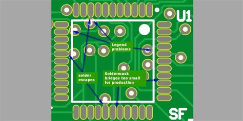
QFP solder bridging is a defect that occurs when excess solder accumulates between adjacent leads of a QFP package, creating an unintended electrical connection. This unwanted connection can cause short circuits, leading to device malfunction or failure.
Causes of QFP Solder Bridging
Several factors can contribute to the occurrence of QFP solder bridging:
-
Excessive solder paste: Applying too much solder paste to the pads can result in excess solder flowing between the leads during reflow, causing bridging.
-
Incorrect stencil design: A poorly designed solder paste stencil with oversized or misaligned apertures can lead to excessive solder paste deposition.
-
Inadequate lead-to-pad alignment: Misalignment between the QFP package leads and the PCB pads can cause solder to bridge between adjacent leads.
-
Inappropriate reflow profile: An incorrect reflow temperature profile, such as excessive peak temperature or insufficient time above liquidus, can cause solder to flow excessively and bridge between leads.
-
Contamination: Presence of contaminants, such as flux residue or foreign particles, can contribute to solder bridging by altering the surface tension of molten solder.
Strategies to Prevent QFP Solder Bridging
Proper Solder Paste Stencil Design
A well-designed solder paste stencil is crucial for achieving optimal solder paste deposition and minimizing the risk of bridging. Consider the following guidelines:
-
Aperture size: Ensure that the stencil apertures are appropriately sized for the QFP package pads. Oversized apertures can lead to excessive solder paste deposition.
-
Aperture shape: Use rectangular or home plate-shaped apertures for QFP pads to promote uniform solder paste distribution and minimize bridging.
-
Stencil thickness: Select an appropriate stencil thickness based on the lead pitch and solder paste particle size. Thinner stencils (e.g., 4-5 mils) are recommended for fine-pitch QFP packages.
| QFP Lead Pitch | Recommended Stencil Thickness |
|---|---|
| 0.5 mm | 4-5 mils (100-125 μm) |
| 0.4 mm | 4 mils (100 μm) |
| 0.3 mm | 3-4 mils (75-100 μm) |
Accurate Component Placement
Precise alignment of the QFP package leads with the PCB pads is essential to prevent solder bridging. Employ the following techniques to ensure accurate component placement:
-
Vision-based alignment: Use machine vision systems or cameras to verify the alignment of the QFP package leads with the PCB pads before soldering.
-
Placement pressure: Apply appropriate placement pressure to ensure that the QFP package is seated flush against the PCB surface, minimizing the risk of lead misalignment.
-
Placement speed: Adjust the placement speed to allow sufficient time for the QFP package to settle onto the solder paste without causing misalignment.
Optimized Reflow Profile
A well-controlled reflow profile is critical for achieving reliable solder joints and minimizing the occurrence of solder bridging. Consider the following guidelines:
-
Peak temperature: Ensure that the peak reflow temperature is within the recommended range for the solder paste and QFP package. Excessive peak temperatures can cause solder to flow excessively and bridge between leads.
-
Time above liquidus (TAL): Maintain an appropriate TAL to allow sufficient time for the solder to wet the surfaces and form reliable joints without excessive flow.
-
Ramp rates: Control the heating and cooling ramp rates to minimize thermal stress on the components and prevent rapid solder flow that can lead to bridging.
| Reflow Profile Parameter | Recommended Value |
|---|---|
| Peak Temperature | 235-245°C |
| Time Above Liquidus | 60-90 seconds |
| Heating Ramp Rate | 1-3°C/second |
| Cooling Ramp Rate | 1-4°C/second |
Flux Selection and Application
The choice of flux and its application method can significantly impact the occurrence of solder bridging. Consider the following recommendations:
-
Flux type: Select a flux with appropriate activity level and compatibility with the solder paste and PCB surface finish. No-clean fluxes are commonly used for QFP soldering to minimize residue and reduce the risk of bridging.
-
Flux application: Apply flux judiciously to the QFP package leads and PCB pads. Excessive flux can contribute to solder bridging by altering the surface tension of molten solder.
-
Flux residue cleaning: If using a water-soluble or rosin-based flux, ensure thorough cleaning of flux residues after soldering to prevent contamination and potential bridging in subsequent reflow cycles.
Inspection and Rework
Post-soldering inspection and rework are essential for identifying and correcting any instances of QFP solder bridging. Implement the following practices:
-
Visual inspection: Perform a visual inspection of the soldered QFP packages using magnification to identify any solder bridges.
-
Automated optical inspection (AOI): Employ AOI systems to detect solder bridging and other soldering defects automatically.
-
Rework techniques: If solder bridging is detected, use appropriate rework techniques, such as solder wick or a hot air rework station, to remove the excess solder and restore the proper electrical isolation between leads.

Frequently Asked Questions (FAQ)
-
What is the main cause of QFP solder bridging?
The main cause of QFP solder bridging is excessive solder paste deposition, which can occur due to incorrect stencil design, improper solder paste application, or inappropriate reflow profile. -
How can I prevent QFP solder bridging during the assembly process?
To prevent QFP solder bridging, ensure proper solder paste stencil design, accurate component placement, optimized reflow profile, and appropriate flux selection and application. Implementing these strategies can significantly reduce the occurrence of solder bridging. -
What is the recommended stencil thickness for a 0.4 mm pitch QFP package?
For a 0.4 mm pitch QFP package, the recommended stencil thickness is 4 mils (100 μm). This thickness ensures adequate solder paste deposition while minimizing the risk of solder bridging. -
How can I detect QFP solder bridging after the soldering process?
QFP solder bridging can be detected through visual inspection using magnification or by employing automated optical inspection (AOI) systems. These methods allow for the identification of solder bridges and other soldering defects. -
What are the consequences of QFP solder bridging if left uncorrected?
If QFP solder bridging is left uncorrected, it can lead to short circuits, device malfunction, or complete failure. Solder bridges can cause unintended electrical connections between adjacent leads, compromising the functionality and reliability of the electronic assembly.

Conclusion
QFP solder bridging is a common challenge encountered in surface-mount assembly, particularly due to the fine pitch and close lead spacing of QFP packages. By understanding the causes of solder bridging and implementing appropriate prevention strategies, such as proper stencil design, accurate component placement, optimized reflow profile, and effective flux management, the occurrence of QFP solder bridging can be significantly minimized.
Regular inspection and rework processes are crucial for identifying and correcting any instances of solder bridging, ensuring the reliability and functionality of the electronic assembly. By adopting best practices and continuously monitoring the soldering process, manufacturers can achieve high-quality and reliable QFP soldering results, minimizing the risk of device failure and enhancing overall product quality.

Leave a Reply