What is a Gerber File?
Gerber files, also known as Gerber X2 or Extended Gerber format, are the most widely used data format to describe the printed circuit board images: copper layers, solder mask, legend, etc.
A Gerber file is a 2D binary vector image description format: it basically contains coordinates and draws lines and areas. It does not have any information about the PCB’s materials or functionality, just the pure geometry.
Gerber files are usually “zipped” into a single archive that contains all the files needed for manufacturing. The PCB fabricator will then load the Gerber files into their CAM (computer-aided manufacturing) software to generate the instructions for the PCB milling, etching, drilling and printing machines.
Anatomy of a Gerber Archive
A typical Gerber archive will contain the following files:
| File Extension | Layer |
|---|---|
| .GTO | Top Overlay (silkscreen) |
| .GTP | Top Paste Mask |
| .GTS | Top Solder Mask |
| .GTL | Top Copper |
| .G1 … .Gn | Inner Copper Layers |
| .GBL | Bottom Copper |
| .GBS | Bottom Solder Mask |
| .GBP | Bottom Paste Mask |
| .GBO | Bottom Overlay (silkscreen) |
| .GM1 | Board Outline |
| .TXT | Drill File |
The Top and Bottom Copper files (.GTL and .GBL) contain the actual copper traces and pads for the top and bottom layers of the board. The solder mask and silkscreen layers work like “stencils” that determine where the solder mask coating and silkscreen ink will be applied. The drill file contains the locations and sizes of all the drill holes.
Multi-layer boards will have additional inner copper layers labeled .G1, .G2, etc. Some designs may also have special purpose layers like solder paste and peelable mask. The board outline layer defines the shape and size of the final board.
Step-by-Step: AutoCAD to Gerber
Now let’s go through the process of actually generating the Gerber files from an AutoCAD PCB design. We’ll assume you’ve already completed the PCB layout and are ready to generate files for manufacturing.
1. Check the design
Before generating Gerber files, it’s important to double-check the PCB design for any errors. Common issues to look for include:
- Traces or pads too close together (shorts)
- Traces or pads not properly connected
- Incorrectly sized pads or drill holes
- Text errors in the silkscreen
- Clearance violations with keep-out areas
- Mismatch between schematic and PCB
Catching and fixing errors at this stage will save time and headaches later in the manufacturing process. Use AutoCAD’s design rule checks (DRC) to automatically verify the PCB meets your specified design constraints.
2. Set up layers
In AutoCAD, the PCB design will be divided into separate layers for the copper, solder mask, silkscreen, drill holes, etc. Make sure all the required layers are present and clearly labeled.
Here’s a sample layer setup for a 2-layer board:
| AutoCAD Layer | Gerber File |
|---|---|
| DIMENSION | .GM1 (Board Outline) |
| MECH1 | .GM2 (Mechanical Layer 1) |
| MECH2 | .GM3 (Mechanical Layer 2) |
| TOP | .GTL (Top Copper) |
| BOTTOM | .GBL (Bottom Copper) |
| SSTOP | .GTO (Top Silkscreen) |
| SSBOT | .GBO (Bottom Silkscreen) |
| SMTOP | .GTS (Top Solder Mask) |
| SMBOT | .GBS (Bottom Solder Mask) |
| THRU | .TXT (Drill Plated Through Holes) |
| NPTH | .TXT (Drill Non-Plated Holes) |
Make sure all objects are placed on the correct AutoCAD layer. For example, all top copper pads and traces should be on the TOP layer.
3. Run Gerber export
With the design checked and layers set up properly, you’re ready to generate the actual Gerber files. In AutoCAD, use the PLOT command to bring up the Plot dialog box.
Under “Printer/plotter”, select the pcb_fab.pc5 driver (this may need to be downloaded and installed first). Then click the Properties button and go to the Device and Document Settings tab.
In the Plot dialog box, set the following Gerber export options:
- Plot scale: 1:1
- Plot area: Window (select the board outline)
- Plot offset: Center the plot
- Plot options:
- Plot with lineweights
- Plot paperspace last
- Hide paperspace objects
Next, go to the layers tab in the Plot dialog box. Here we’ll select which AutoCAD layers to include in the Gerber export. For each copper, mask, or silkscreen layer you want to export:
- Select the AutoCAD layer
- Set the plot style to GERBER
- Check the “Plot” box
For example, to export the top copper layer, select the TOP AutoCAD layer, set the plot style to GERBER, and check Plot. Repeat this for all the required layers (BOTTOM, SSTOP, SMTOP, etc.)
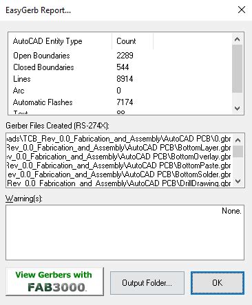
When you’ve selected all the layers to export, click OK to run the Gerber export process. AutoCAD will generate a separate Gerber file for each layer selected.
4. Generate drill file
In addition to the Gerber files, you’ll also need to provide the drill file to the manufacturer. The drill file specifies the sizes and locations of all the drilled holes in the board.
To generate the drill file in AutoCAD:
- Type ATTEDIT on the command line
- Select the drill holes (plated or non-plated)
- Right-click and select Properties
- Go to the Attributes tab
- Click the Export Hole Table button
- Save the drill file in Excellon format (.TXT)
5. Review Gerber output
After exporting the Gerber and drill files, it’s a good idea to quickly review them for any obvious errors. Most PCB manufacturers will provide a free Gerber viewer tool on their website.
Upload your Gerber archive (ZIP file) to the viewer and check for issues like:
- Missing layers
- Incorrect board outline
- Drill holes not aligned to pads
- Incorrect pad or trace sizes
- Missing solder mask openings
Reviewing the Gerber files in a viewer is much easier than trying to inspect the raw Gerber code. If you spot any problems, go back and fix them in the AutoCAD design, then re-export the Gerber files.
6. Send to manufacturer
With your Gerber files generated and verified, you’re ready to send them to the PCB manufacturer for fabrication. Most manufacturers will ask you to upload the Gerber ZIP file on their website or send it via email.
In addition to the Gerbers, you’ll also need to provide some additional information like:
- PCB quantity
- Layer count
- Material type (FR-4, etc.)
- Copper weight
- Surface finish (HASL, ENIG, etc.)
- Solder mask color
- Silkscreen color
- Any special requirements
The manufacturer will then analyze your Gerber data and provide a quote for the PCB fabrication. After you approve the quote and place the order, they’ll proceed with manufacturing your PCBs!

FAQ
Can I send my AutoCAD PCB design directly to a manufacturer without Gerbers?
In general, no. While a few manufacturers may accept AutoCAD DXF or DWG files, the vast majority will require standard RS-274X Gerber files for fabrication. Gerber is the lingua franca of PCB manufacturing.
What if I don’t have the pcb_fab.pc5 Gerber driver installed?
The pcb_fab.pc5 driver is a plotter driver that configures AutoCAD to export in Extended Gerber X2 format. If you don’t have it installed, you can download it from various PCB design websites or software vendors. As an alternative, you can also use a third-party Gerber export macro or script for AutoCAD.
What’s the difference between Gerber X1 and X2 format?
Gerber X1 (aka RS-274D) is an older Gerber format that is now considered obsolete. It has some limitations like no support for apertures or drill holes. Extended Gerber or X2 format (aka RS-274X) added features like custom apertures, positive/negative polarity, and new G-codes. Always export Gerber X2 unless your manufacturer specifically requests otherwise.
How do I check my Gerber files for errors?
Most PCB manufacturers provide free online Gerber viewer tools that will display your PCB design and highlight common issues. For a more thorough analysis, standalone Gerber viewer applications like gerbv, GC-Prevue, and ViewMate offer additional features like design rule checks and layer compare.
The manufacturer says there’s a problem with my Gerber files. What do I do?
If the PCB fabricator reports an issue with your Gerber data, the first step is to identify which layer(s) are causing the problem. Open the affected files in a Gerber viewer and look for obvious issues like incorrect apertures, open traces, or invalid G-codes.
If you can’t spot the problem visually, compare the Gerber files against your original AutoCAD design to see if there are any differences. Common export issues include selecting the wrong layers, using non-standard apertures, or incorrect units.
Once you’ve identified and fixed the issue in AutoCAD, re-generate the Gerber files and send them to the manufacturer for a new analysis. It’s not uncommon to go through a couple of iterations before the Gerbers are perfect.

Conclusion
Generating manufacturing-quality Gerber files is a key skill for any PCB designer. By following the steps in this guide, you’ll be able to quickly and easily export your AutoCAD PCB layouts in extended Gerber X2 format, ready for fabrication.
While the Gerber export process is not overly complicated, it does require attention to detail. Always double-check your designs before generating Gerbers, and carefully review the exported files in a Gerber viewer. If you can provide clean, error-free Gerber files to your manufacturer, you’ll avoid production delays and get your PCBs manufactured faster.
The PCB design and manufacturing process doesn’t have to be a black box. By learning to speak the language of Gerber, you can communicate your designs effectively and collaborate with your manufacturing partners to bring your electronic products to life!

Leave a Reply