What are Gerber Files?
Gerber files are a standard file format used in the printed circuit board (PCB) industry to describe the layout of a PCB. They contain all the necessary information for manufacturing, including the copper layers, solder mask, silk screen, and drill holes. Gerber files are essential for communicating your PCB design to a manufacturer and ensuring that your board is produced accurately.
Why Export to Gerber?
Exporting your KiCad PCB design to Gerber files is crucial for several reasons:
-
Manufacturing: Gerber files are the industry standard for PCB Fabrication. Manufacturers require Gerber files to produce your PCB accurately.
-
Compatibility: Gerber files are compatible with a wide range of PCB manufacturing equipment and software, ensuring that your design can be produced by most manufacturers.
-
Quality Control: Gerber files allow you to review and verify your PCB layout before sending it for manufacturing, reducing the risk of errors and ensuring a high-quality final product.

Preparing Your KiCad PCB for Gerber Export
Before exporting your KiCad PCB to Gerber files, it’s essential to ensure that your design is complete and error-free. Follow these steps to prepare your PCB:
-
Design Rule Check (DRC): Run a DRC to identify any design rule violations, such as incorrect trace widths, spacing issues, or missing connections. Fix any errors before proceeding.
-
Electrical Rule Check (ERC): Perform an ERC to detect any electrical issues, such as unconnected pins, shorted nets, or missing power connections. Address any problems found during the ERC.
-
Board Outline: Ensure that your PCB has a clearly defined board outline. This outline will be used to create the Gerber files and determine the final shape of your PCB.
-
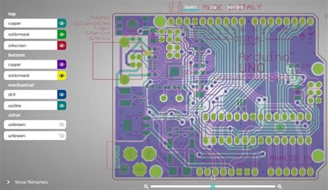
Copper Layers: Verify that all copper layers are correctly assigned and named. This includes the top and bottom layers, as well as any inner layers if you have a multi-layer PCB.
-
Silk Screen: Check that your silk screen layer contains all the necessary information, such as component outlines, labels, and logos. Make sure the text is legible and properly positioned.
-
Solder Mask: Review your solder mask layer to ensure that it correctly covers the areas where you don’t want solder to be applied, such as between closely spaced pads.
-
Drill Files: Confirm that all drill holes are correctly defined, including the hole sizes and locations. KiCad will generate a separate drill file during the Gerber export process.

Exporting Gerber Files from KiCad
Once your KiCad PCB is prepared, follow these steps to export your design to Gerber files:
-
Open your KiCad PCB project and navigate to the “File” menu.
-
Select “Plot” from the dropdown menu. This will open the Gerber file generation dialog.
-
In the “Plot” dialog, select the folder where you want to save your Gerber files.
-
Choose the appropriate Gerber file format. The most common format is “Gerber RS-274X.”
-
Select the layers you want to include in your Gerber files. Typically, you’ll need to include the following layers:
- Top Copper (F.Cu)
- Bottom Copper (B.Cu)
- Top Solder Mask (F.Mask)
- Bottom Solder Mask (B.Mask)
- Top Silk Screen (F.SilkS)
- Bottom Silk Screen (B.SilkS)
-
Board Outline (Edge.Cuts)
-
Adjust any other settings as needed, such as the plot format and line width.
-
Click “Plot” to generate the Gerber files. KiCad will create a separate file for each layer you selected.
-
To generate the drill files, click “Generate Drill Files” in the “Plot” dialog.
-
Choose the appropriate drill file format, such as “Excellon,” and click “Generate Drill File.”
-
Review the generated Gerber and drill files to ensure they are complete and accurate.

Verifying Gerber Files
After generating your Gerber files, it’s crucial to verify them before sending them to a manufacturer. There are several tools available for checking Gerber files, including:
-
GerbView: A free Gerber viewer included with KiCad that allows you to inspect your Gerber files visually.
-
Online Gerber Viewers: Many PCB manufacturers offer online Gerber viewers that allow you to upload and review your files before placing an order.
-
Third-Party Gerber Viewers: There are various third-party Gerber viewers available, such as ViewMate and CAM350, which provide advanced features for analyzing and verifying Gerber files.
When verifying your Gerber files, look for the following:
-
Layer Alignment: Ensure that all layers are correctly aligned and that there are no unintended offsets or rotations.
-
Apertures: Check that all apertures (pads, traces, and other features) are correctly defined and sized.
-
Drill Holes: Verify that all drill holes are present and correctly positioned.
-
Board Outline: Confirm that the board outline is correctly defined and matches your intended PCB shape.
-
Manufacturability: Review your Gerber files for any potential manufacturing issues, such as thin traces, small clearances, or unsupported features.
Sending Gerber Files to a Manufacturer
Once you have verified your Gerber files, you can send them to a PCB manufacturer for production. When communicating with a manufacturer, provide the following information:
-
Gerber Files: Include all the necessary Gerber files, typically in a compressed ZIP folder.
-
Drill Files: Include the drill files generated by KiCad, usually in Excellon format.
-
PCB Specifications: Provide details about your PCB, such as the dimensions, thickness, copper weight, solder mask color, and silk screen color.
-
Quantity: Specify the number of PCBs you need to be manufactured.
-
Special Requirements: If you have any special requirements, such as surface finish, impedance control, or controlled impedance, make sure to communicate these to the manufacturer.
Most PCB manufacturers have an online quoting system where you can upload your Gerber files and specify your requirements. They will then provide you with a quote and lead time for your order.
Frequently Asked Questions (FAQ)
- What are the most common mistakes when exporting Gerber files from KiCad?
- Forgetting to include all necessary layers
- Not defining the board outline correctly
- Failing to generate drill files
-
Not verifying the Gerber files before sending them to a manufacturer
-
Can I export Gerber files from KiCad for a multi-layer PCB?
Yes, KiCad supports exporting Gerber files for multi-layer PCBs. Make sure to include all the necessary copper layers and inner layers when selecting the layers to export. -
What should I do if my Gerber files are rejected by a manufacturer?
If a manufacturer rejects your Gerber files, request specific feedback on the issues they encountered. Review your files and make the necessary corrections based on their feedback. If you’re unsure how to resolve the issues, consult the KiCad community or a PCB design expert for assistance. -
Can I use Gerber files generated by KiCad with any PCB manufacturer?
Yes, Gerber files are an industry standard and should be compatible with most PCB manufacturers. However, it’s always a good idea to check with your chosen manufacturer to ensure they accept Gerber files generated by KiCad. -
How can I ensure my Gerber files are correctly generated and error-free?
To minimize the risk of errors in your Gerber files: - Follow the preparation steps outlined earlier, including running DRC and ERC checks
- Carefully review and verify your Gerber files using a Gerber viewer
- Double-check that you have included all necessary layers and files
- Communicate clearly with your manufacturer and provide all required information
| Step | Description |
|---|---|
| 1 | Open your KiCad PCB project and navigate to the “File” menu |
| 2 | Select “Plot” from the dropdown menu |
| 3 | In the “Plot” dialog, select the folder where you want to save your Gerber files |
| 4 | Choose the appropriate Gerber file format (e.g., Gerber RS-274X) |
| 5 | Select the layers to include in your Gerber files |
| 6 | Adjust any other settings as needed |
| 7 | Click “Plot” to generate the Gerber files |
| 8 | Click “Generate Drill Files” in the “Plot” dialog |
| 9 | Choose the appropriate drill file format (e.g., Excellon) and click “Generate Drill File” |
| 10 | Review the generated Gerber and drill files for accuracy |
By following this comprehensive guide, you should be well-equipped to export your KiCad PCB designs to Gerber files and communicate effectively with PCB manufacturers. Remember to always verify your files and provide clear instructions to ensure a smooth and successful PCB manufacturing process.
Leave a Reply