Introduction to Goldfinger PCB
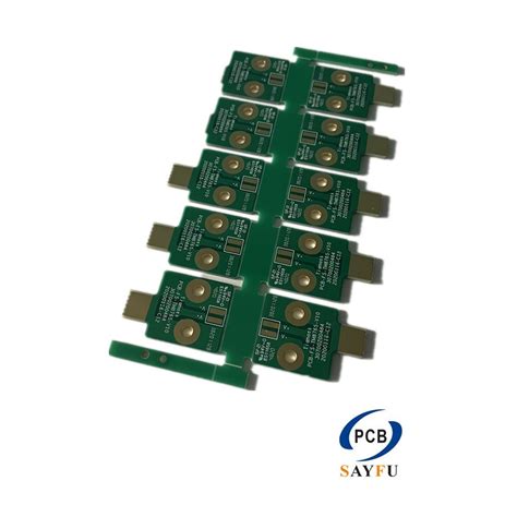
Goldfinger PCB, also known as gold plated printed circuit boards, are widely used in various industries due to their superior electrical conductivity, excellent corrosion resistance, and high reliability. These PCBs are manufactured by depositing a thin layer of gold on the copper traces and pads of the board, ensuring optimal performance in demanding applications such as aerospace, military, and medical devices.
However, despite the numerous advantages of Goldfinger PCBs, manufacturers often face quality issues that can compromise the functionality and longevity of the final product. This article will explore the common quality issues associated with Goldfinger PCBs and discuss effective measures to mitigate these problems.
The Importance of Gold Plating in PCBs
Gold plating plays a crucial role in enhancing the performance and durability of printed circuit boards. The primary reasons for using gold plating in PCBs include:
-
Enhanced electrical conductivity: Gold is an excellent conductor of electricity, ensuring minimal signal loss and improved signal integrity.
-
Corrosion resistance: Gold is highly resistant to oxidation and corrosion, protecting the underlying copper traces from environmental factors that can degrade performance over time.
-
Improved solderability: Gold-plated surfaces offer excellent solderability, facilitating the assembly process and ensuring robust solder joints.
-
Reduced contact resistance: Gold plating minimizes contact resistance between mating surfaces, such as connectors and switches, resulting in more reliable connections.

Common Quality Issues in Goldfinger PCBs
Despite the benefits of gold plating, Goldfinger PCBs are susceptible to various quality issues that can affect their performance and reliability. Some of the most common quality issues include:
1. Inadequate Gold Thickness
One of the primary quality issues in Goldfinger PCBs is inadequate gold thickness. When the gold plating is too thin, it may not provide sufficient protection against corrosion and wear, leading to premature failure of the PCB. On the other hand, excessive gold thickness can cause issues such as embrittlement and reduced flexibility of the board.
To ensure optimal performance, it is essential to maintain the appropriate gold thickness based on the specific application requirements. The following table provides a general guideline for gold thickness in various applications:
| Application | Recommended Gold Thickness |
|---|---|
| Wire bonding | 0.5 – 1.5 μm |
| Soldering | 0.05 – 0.5 μm |
| Connector contacts (low mating cycles) | 0.2 – 0.8 μm |
| Connector contacts (high mating cycles) | 0.8 – 1.5 μm |
2. Porosity and Pinholes
Porosity and pinholes in the gold plating can compromise the protective properties of the coating, exposing the underlying copper to corrosion and contamination. These defects can occur due to various factors, such as:
- Improper surface preparation before plating
- Inadequate cleaning of the PCB during the plating process
- Incorrect plating parameters (e.g., current density, temperature, and pH)
- Contamination of the plating solution
To minimize porosity and pinholes, manufacturers should implement strict process controls and regularly monitor the plating solution for contaminants.
3. Adhesion Issues
Poor adhesion between the gold plating and the underlying copper can lead to delamination and peeling of the gold layer, exposing the copper to corrosion and reducing the reliability of the PCB. Adhesion issues can arise due to:
- Inadequate surface preparation, such as insufficient cleaning or roughening of the copper surface
- Incompatible plating chemistries or processes
- Stress induced by thermal expansion mismatches between the gold and copper layers
To improve adhesion, manufacturers should optimize surface preparation techniques, select compatible plating chemistries, and control the plating process parameters to minimize stress.
4. Contamination
Contamination of the gold plating can occur during various stages of the manufacturing process, such as handling, storage, and assembly. Common contaminants include:
- Organic residues from cleaning agents or flux
- Metallic particles from the manufacturing environment
- Oxides and sulfides formed during the plating process
Contamination can lead to reduced electrical conductivity, poor solderability, and decreased reliability of the PCB. To prevent contamination, manufacturers should implement strict cleanliness standards, use high-purity plating solutions, and store Goldfinger PCBs in controlled environments.

Measures to Improve Goldfinger PCB Quality
To address the quality issues associated with Goldfinger PCBs, manufacturers can implement several measures:
1. Process Optimization
Optimizing the gold plating process is crucial for ensuring consistent and high-quality results. This involves:
- Selecting the appropriate plating chemistry and additives
- Controlling the plating parameters, such as current density, temperature, and pH
- Regularly monitoring and maintaining the plating solution to prevent contamination
- Implementing statistical process control (SPC) to identify and correct process deviations
2. Surface Preparation
Proper surface preparation is essential for achieving good adhesion and minimizing defects in the gold plating. Key steps in surface preparation include:
- Cleaning the PCB to remove contaminants and oxides
- Microetching or roughening the copper surface to improve adhesion
- Applying a suitable acid cleaner or activator to ensure uniform plating
3. Quality Control and Inspection
Implementing robust quality control and inspection procedures can help identify and address quality issues early in the manufacturing process. This may include:
- Visual inspection of the PCB surface for defects such as pinholes, blisters, and discoloration
- Thickness measurement using X-ray fluorescence (XRF) or beta backscatter techniques
- Adhesion testing using tape tests or peel tests
- Electrical testing to verify conductivity and signal integrity
4. Supplier Management
Collaborating with reliable suppliers of plating chemicals, equipment, and materials can help ensure consistent quality in Goldfinger PCBs. Manufacturers should:
- Qualify suppliers based on their technical expertise, quality management systems, and track record
- Establish clear specifications and quality requirements for purchased materials
- Conduct regular audits and performance evaluations of suppliers
5. Training and Education
Investing in training and education for personnel involved in the manufacturing of Goldfinger PCBs can help improve quality and reduce defects. This may include:
- Providing technical training on plating processes, quality control, and inspection methods
- Encouraging cross-functional collaboration between design, manufacturing, and quality teams
- Fostering a culture of continuous improvement and problem-solving

Frequently Asked Questions (FAQ)
-
What is the purpose of gold plating in PCBs?
Gold plating in PCBs serves several purposes, including enhancing electrical conductivity, improving corrosion resistance, facilitating solderability, and reducing contact resistance. -
How does gold thickness affect the performance of Goldfinger PCBs?
The gold thickness in Goldfinger PCBs should be optimized based on the specific application requirements. Insufficient gold thickness may not provide adequate protection against corrosion and wear, while excessive thickness can lead to embrittlement and reduced flexibility. -
What are the common causes of porosity and pinholes in gold plating?
Porosity and pinholes in gold plating can occur due to improper surface preparation, inadequate cleaning during the plating process, incorrect plating parameters, and contamination of the plating solution. -
How can adhesion issues between the gold plating and copper be prevented?
Adhesion issues can be prevented by optimizing surface preparation techniques, selecting compatible plating chemistries, and controlling the plating process parameters to minimize stress. -
What measures can manufacturers take to improve the quality of Goldfinger PCBs?
Manufacturers can improve the quality of Goldfinger PCBs by optimizing the plating process, implementing proper surface preparation, conducting robust quality control and inspection, collaborating with reliable suppliers, and investing in training and education for personnel.
Conclusion
Goldfinger PCBs offer numerous benefits, including enhanced electrical conductivity, corrosion resistance, and improved solderability. However, manufacturers must address various quality issues, such as inadequate gold thickness, porosity, pinholes, adhesion problems, and contamination, to ensure optimal performance and reliability.
By implementing measures such as process optimization, surface preparation, quality control, supplier management, and training, manufacturers can significantly improve the quality of Goldfinger PCBs and meet the demanding requirements of industries such as aerospace, military, and medical devices.
As technology advances and applications become more complex, the importance of high-quality Goldfinger PCBs will only continue to grow. By understanding the common quality issues and adopting best practices for manufacturing, suppliers can position themselves as reliable partners in the development of cutting-edge electronic products.
Leave a Reply