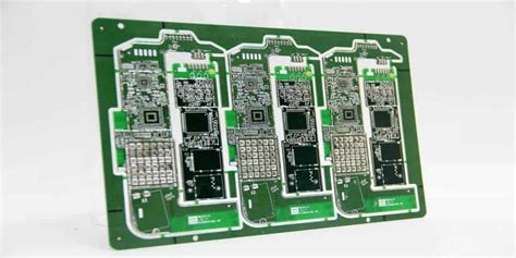
Introduction to Goldfinger PCBs
Goldfinger PCBs, also known as gold plated printed circuit boards, are a type of high-quality PCB that uses a layer of gold plating over the copper traces and pads. The gold plating provides several benefits, including improved corrosion resistance, better electrical conductivity, and enhanced solderability. These advantages make Goldfinger PCBs ideal for applications that require high reliability, such as aerospace, military, and medical devices.
However, despite the superior characteristics of gold plated PCBs, they are not immune to quality issues. In this article, we will discuss some of the common quality problems associated with Goldfinger PCBs and the measures that can be taken to address them.
Common Quality Issues in Goldfinger PCBs
Inadequate Gold Plating Thickness
One of the most critical aspects of Goldfinger PCBs is the thickness of the gold plating. If the gold layer is too thin, it may not provide sufficient protection against corrosion or enhance the electrical properties of the board. On the other hand, if the gold plating is too thick, it can lead to issues such as poor adhesion, excessive cost, and difficulties in soldering.
The ideal gold plating thickness depends on the specific application and the requirements of the end-user. The following table provides a general guideline for gold plating thickness based on the intended use:
| Application | Recommended Gold Plating Thickness |
|---|---|
| General-purpose | 0.05-0.1 µm |
| High-reliability (aerospace) | 0.2-0.5 µm |
| Wire bonding | 0.8-1.2 µm |
To ensure adequate gold plating thickness, manufacturers should employ strict process controls and regular inspections using techniques such as X-ray fluorescence (XRF) or cross-sectional analysis.
Gold Plating Porosity
Porosity in the gold plating layer can lead to several issues, such as reduced corrosion resistance, poor electrical conductivity, and decreased solderability. Pores in the gold layer can allow moisture and contaminants to reach the underlying copper, leading to corrosion and degradation of the PCB’s performance over time.
Several factors can contribute to gold plating porosity, including:
- Improper surface preparation before plating
- Contamination in the plating solution
- Incorrect plating parameters (e.g., current density, temperature)
- Inadequate post-plating cleaning and drying
To minimize porosity, manufacturers should implement strict process controls, use high-quality plating solutions, and perform regular maintenance on the plating equipment. Additionally, post-plating inspections using techniques such as scanning electron microscopy (SEM) can help identify porosity issues.
Gold Plating Adhesion
Poor adhesion between the gold plating and the underlying copper can lead to delamination, which can cause electrical failures and reliability issues. Factors that can contribute to poor adhesion include:
- Inadequate surface cleaning and preparation
- Contamination on the copper surface
- Incorrect plating parameters
- Stress induced by thermal cycling or mechanical stress
To improve gold plating adhesion, manufacturers should follow best practices for surface preparation, such as proper cleaning and etching of the copper surface. Additionally, the use of a nickel underplating layer can help improve the adhesion between the gold and copper.
Solder Wettability Issues
Gold plated PCBs can sometimes experience issues with solder wettability, which can lead to poor solder joint quality and reliability. Factors that can contribute to solder wettability issues include:
- Excessive gold plating thickness
- Contamination on the gold surface
- Oxidation of the gold surface
- Incorrect soldering parameters (e.g., temperature, time)
To address solder wettability issues, manufacturers should control the gold plating thickness, ensure proper storage and handling of the PCBs to prevent contamination and oxidation, and optimize the soldering process parameters.

Measures to Improve Goldfinger PCB Quality
Strict Process Controls
Implementing strict process controls throughout the manufacturing process is essential for ensuring the quality of Goldfinger PCBs. This includes:
- Proper storage and handling of materials
- Regular maintenance and calibration of equipment
- Detailed work instructions and operator training
- In-process inspections and quality checks
By adhering to well-defined processes and monitoring key parameters, manufacturers can minimize the occurrence of quality issues and ensure consistent performance of the gold plated PCBs.
Advanced Inspection Techniques
Employing advanced inspection techniques can help identify quality issues early in the manufacturing process, allowing for timely corrective actions. Some of the key inspection techniques for Goldfinger PCBs include:
- X-ray fluorescence (XRF) for measuring gold plating thickness
- Scanning electron microscopy (SEM) for evaluating plating porosity and adhesion
- Cross-sectional analysis for assessing plating thickness and uniformity
- Solderability testing for evaluating solder wettability
By incorporating these inspection techniques into the quality control process, manufacturers can detect and address quality issues before they impact the end product.
Continuous Improvement Initiatives
Implementing continuous improvement initiatives can help manufacturers identify and eliminate the root causes of quality issues in Goldfinger PCBs. This can involve:
- Collecting and analyzing process and quality data
- Conducting root cause analysis for recurring quality issues
- Implementing corrective and preventive actions (CAPAs)
- Engaging employees in problem-solving and improvement activities
By fostering a culture of continuous improvement, manufacturers can proactively address quality issues and drive ongoing enhancements in the performance and reliability of gold plated PCBs.

Frequently Asked Questions (FAQ)
-
What are the benefits of using Goldfinger PCBs compared to standard PCBs?
Goldfinger PCBs offer several advantages over standard PCBs, including improved corrosion resistance, better electrical conductivity, and enhanced solderability. These properties make them ideal for applications that require high reliability and performance, such as aerospace, military, and medical devices. -
How does the gold plating thickness affect the performance of Goldfinger PCBs?
The gold plating thickness plays a crucial role in the performance of Goldfinger PCBs. If the gold layer is too thin, it may not provide sufficient protection against corrosion or enhance the electrical properties of the board. Conversely, if the gold plating is too thick, it can lead to issues such as poor adhesion, excessive cost, and difficulties in soldering. The ideal gold plating thickness depends on the specific application and the requirements of the end-user. -
What are some common causes of gold plating porosity in Goldfinger PCBs?
Several factors can contribute to gold plating porosity, including improper surface preparation before plating, contamination in the plating solution, incorrect plating parameters (e.g., current density, temperature), and inadequate post-plating cleaning and drying. To minimize porosity, manufacturers should implement strict process controls, use high-quality plating solutions, and perform regular maintenance on the plating equipment. -
How can manufacturers improve the adhesion between the gold plating and the underlying copper in Goldfinger PCBs?
To improve gold plating adhesion, manufacturers should follow best practices for surface preparation, such as proper cleaning and etching of the copper surface. Additionally, the use of a nickel underplating layer can help improve the adhesion between the gold and copper. Strict process controls and regular inspections can also help ensure consistent adhesion quality. -
What measures can manufacturers take to address solder wettability issues in Goldfinger PCBs?
To address solder wettability issues, manufacturers should control the gold plating thickness, ensure proper storage and handling of the PCBs to prevent contamination and oxidation, and optimize the soldering process parameters. Regular solderability testing can also help identify and correct any wettability issues before they impact the end product.

Conclusion
Goldfinger PCBs offer superior performance and reliability compared to standard PCBs, making them an ideal choice for demanding applications. However, they are not immune to quality issues, such as inadequate gold plating thickness, porosity, poor adhesion, and solder wettability problems. By implementing strict process controls, advanced inspection techniques, and continuous improvement initiatives, manufacturers can proactively address these quality issues and ensure the consistent performance of gold plated PCBs. As the demand for high-reliability electronic devices continues to grow, the importance of maintaining the highest quality standards in Goldfinger PCB manufacturing will only increase.
Leave a Reply