Introduction to RAYPCB and Laser Direct Imaging
RAYPCB is a leading PCB manufacturer that specializes in high-quality, advanced PCB fabrication techniques. One of the key technologies employed by RAYPCB is Laser Direct Imaging (LDI), a process that has revolutionized the PCB industry. In this article, we will delve into the details of LDI, its advantages, and how RAYPCB utilizes this technology to produce superior PCBs.
What is Laser Direct Imaging?
Laser Direct Imaging is a PCB fabrication process that uses a high-powered laser to directly expose the PCB’s photoresist layer. This process eliminates the need for traditional photomasks, which are used in conventional PCB fabrication methods. LDI offers several advantages over traditional methods, including higher precision, improved reliability, and faster turnaround times.
How does Laser Direct Imaging work?
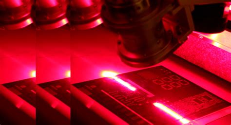
The LDI process begins with the application of a photoresist layer onto the copper-clad PCB substrate. The photoresist is a light-sensitive material that hardens when exposed to UV light. In the LDI process, a high-powered laser is used to selectively expose the photoresist layer, creating the desired circuit pattern directly on the PCB.
The laser used in LDI is typically a UV laser with a wavelength of 355 nm or 405 nm. The laser beam is focused onto the PCB surface and scans across the board, exposing the photoresist in a precise, controlled manner. The exposed areas of the photoresist harden, while the unexposed areas remain soluble and can be easily removed during the development process.
Advantages of Laser Direct Imaging
1. High Precision and Accuracy
One of the primary advantages of LDI is its ability to produce highly precise and accurate PCB patterns. The laser used in LDI can achieve a minimum feature size of around 25 microns, which is significantly smaller than what can be achieved with traditional photomask-based methods. This high precision enables the fabrication of dense, complex PCB designs with fine pitch components.
2. Improved Registration and Alignment
LDI eliminates the need for physical photomasks, which can be prone to misalignment and registration errors. With LDI, the laser directly exposes the photoresist layer, ensuring perfect registration between the PCB layers. This improved alignment results in higher yields and fewer defects, especially in multi-layer PCBs.
3. Faster Turnaround Times
The LDI process is highly automated and efficient, allowing for faster PCB fabrication turnaround times. By eliminating the need for photomasks, LDI reduces the time and costs associated with mask production and maintenance. Additionally, the direct exposure of the photoresist layer streamlines the fabrication process, enabling quicker production runs.
4. Enhanced Flexibility and Adaptability
LDI offers greater flexibility and adaptability compared to traditional PCB fabrication methods. With LDI, design changes can be easily incorporated without the need to produce new photomasks. This flexibility is particularly valuable for prototyping and low-volume production runs, where design iterations are common.
5. Improved Reliability and Consistency
The high precision and accuracy of LDI result in improved reliability and consistency of the fabricated PCBs. The direct exposure of the photoresist layer minimizes the risk of defects and ensures uniform patterning across the entire PCB surface. This consistency translates into higher quality PCBs with better performance and longer lifespans.

RAYPCB’s Laser Direct Imaging Capabilities
RAYPCB has invested in state-of-the-art LDI equipment to provide its customers with the highest quality PCBs. The company’s LDI systems are capable of handling a wide range of PCB sizes and materials, including rigid, flexible, and rigid-flex PCBs.
LDI Equipment and Specifications
RAYPCB’s LDI systems feature high-powered UV lasers with wavelengths of 355 nm and 405 nm. These lasers are capable of achieving a minimum feature size of 25 microns, enabling the fabrication of dense, high-precision PCBs. The LDI equipment is fully automated and can handle PCBs up to 24″ x 30″ in size.
| Specification | Value |
|---|---|
| Laser Wavelength | 355 nm, 405 nm |
| Minimum Feature Size | 25 microns |
| Maximum PCB Size | 24″ x 30″ |
| Supported PCB Types | Rigid, Flexible, Rigid-Flex |
Quality Control and Inspection
To ensure the highest quality PCBs, RAYPCB employs strict quality control measures throughout the LDI process. The company’s experienced technicians monitor the LDI equipment to ensure optimal performance and consistency. Additionally, RAYPCB utilizes advanced inspection tools, such as automated optical inspection (AOI) and 3D scanning, to detect and rectify any defects or irregularities in the fabricated PCBs.
PCB Design Support and Guidance
RAYPCB offers comprehensive PCB design support and guidance to its customers. The company’s team of experienced PCB designers can assist in optimizing PCB layouts for LDI fabrication, ensuring the best possible results. RAYPCB also provides design rule guidelines and recommendations to help customers create LDI-compatible PCB designs.

Applications of Laser Direct Imaging
LDI technology is widely used in various industries and applications that require high-precision, reliable PCBs. Some of the key applications of LDI include:
1. High-Density Interconnect (HDI) PCBs
HDI PCBs are characterized by their fine pitch components, thin traces, and small via sizes. LDI’s high precision and accuracy make it an ideal choice for fabricating HDI PCBs. The technology enables the creation of dense, complex PCB layouts with minimal defects and high yields.
2. Aerospace and Defense Electronics
The aerospace and defense industries require PCBs that can withstand harsh environments and meet stringent reliability standards. LDI’s ability to produce highly precise and consistent PCBs makes it well-suited for these demanding applications. The improved reliability and performance of LDI-fabricated PCBs ensure the proper functioning of critical aerospace and defense systems.
3. Medical Devices and Equipment
Medical devices and equipment often require compact, high-density PCBs with strict quality and reliability requirements. LDI technology enables the fabrication of PCBs that meet these stringent standards, ensuring the safe and effective operation of medical devices. The high precision and consistency of LDI are particularly valuable for implantable medical devices and diagnostic equipment.
4. Automotive Electronics
The automotive industry is increasingly relying on advanced electronic systems for safety, performance, and entertainment features. LDI-fabricated PCBs offer the high precision and reliability needed for automotive applications. The technology’s ability to produce dense, complex PCB layouts enables the integration of more features and functionalities into automotive electronic systems.
5. IoT and Wearable Devices
The Internet of Things (IoT) and wearable device markets require compact, high-performance PCBs that can be produced quickly and efficiently. LDI technology is well-suited for these applications, as it enables the fabrication of small, dense PCBs with fast turnaround times. The flexibility and adaptability of LDI also make it ideal for the rapidly evolving IoT and wearable device markets.

Frequently Asked Questions (FAQ)
-
Q: What is the minimum feature size that can be achieved with RAYPCB’s Laser Direct Imaging technology?
A: RAYPCB’s LDI systems are capable of achieving a minimum feature size of 25 microns. -
Q: Can Laser Direct Imaging be used for both rigid and flexible PCBs?
A: Yes, RAYPCB’s LDI technology can be used to fabricate rigid, flexible, and rigid-flex PCBs. -
Q: How does Laser Direct Imaging improve PCB reliability and consistency?
A: LDI’s high precision and accuracy result in uniform patterning and minimal defects, leading to improved reliability and consistency of the fabricated PCBs. -
Q: What are the advantages of Laser Direct Imaging over traditional PCB fabrication methods?
A: LDI offers several advantages, including higher precision, improved registration and alignment, faster turnaround times, enhanced flexibility, and improved reliability and consistency. -
Q: Does RAYPCB offer PCB design support for Laser Direct Imaging?
A: Yes, RAYPCB’s team of experienced PCB designers can assist in optimizing PCB layouts for LDI fabrication and provide design rule guidelines and recommendations.
Conclusion
Laser Direct Imaging is a cutting-edge PCB fabrication technology that offers numerous advantages over traditional methods. RAYPCB has invested in state-of-the-art LDI equipment and expertise to provide its customers with the highest quality PCBs. The company’s LDI capabilities enable the fabrication of dense, high-precision PCBs with improved reliability and consistency.
By leveraging LDI technology, RAYPCB can support a wide range of industries and applications, from high-density interconnect PCBs to aerospace and defense electronics, medical devices, automotive electronics, and IoT and wearable devices. With its commitment to quality, innovation, and customer support, RAYPCB is well-positioned to meet the evolving needs of the PCB industry.
Leave a Reply