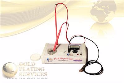
What is a PCB Repair Kit?
A PCB (printed circuit board) repair kit is a set of tools and materials used to fix damaged PCBs. These kits typically include:
- Copper tape or foil for repairing traces
- Insulating tape or paint for covering repairs
- Soldering iron and solder for reconnecting components
- Flux for improving solder connections
- Tweezers, knife, and other tools for precise repairs
- Magnifying glass for inspecting small parts
- Instructions or guides for common repair techniques
PCB repair kits allow technicians and hobbyists to salvage and restore circuit boards that have suffered physical damage, like lifted pads or broken traces. With some skill and patience, a repair kit makes it possible to extend the life of expensive or hard-to-replace PCBs.
When to Use a PCB Repair Kit
Damage to a PCB can occur during assembly, rework, or regular use. Some common issues that may call for a repair include:
| Problem | Description |
|---|---|
| Lifted pad | A pad has detached from the board, breaking its connection |
| Broken trace | A copper trace has cracked or worn away, interrupting the circuit |
| Damaged plating | The protective coating on vias, pads or traces has degraded |
| Burnt component | A component has overheated and needs to be replaced |
In many cases, scrapping a damaged board and making a new one is the best approach. However, repairs can be a good option when:
- The board is expensive or hard to replace
- Only a small area is damaged
- The repair can be made reliably
- Cosmetic flaws are acceptable
- Time is limited for making a new board
A PCB repair kit has the tools to handle physical repairs to the board itself. Diagnosis and replacement of components requires additional tools like a multimeter, oscilloscope, power supply, etc.

How to Use Copper Tape or Foil
One of the most useful items in a PCB repair kit is copper tape or foil. This adhesive-backed copper can be cut to size and applied to the board to replace damaged traces and pads.
Replacing a Lifted Pad
- Clean the area around the lifted pad with isopropyl alcohol.
- Cut a piece of copper tape slightly larger than the pad.
- Stick the tape over the pad location and burnish it down.
- Carefully cut away the excess tape with a sharp knife.
- Solder the component lead to the new copper pad.
Patching a Broken Trace
- Scrape away any solder mask covering the trace ends.
- Clean the area with alcohol.
- Cut a thin strip of copper tape long enough to bridge the gap.
- Carefully stick the tape to the board, covering both trace ends.
- Burnish the tape flat to the board.
- Solder the tape to the trace at both ends.
After making repairs with copper tape, it’s a good idea to cover the repair with insulating tape, epoxy, or conformal coating. This protects the new connection both mechanically and electrically.

Using a Soldering Iron
A soldering iron is used in many PCB repairs for removing and replacing components and connecting new material to the board. Using the right tools and technique is important for making reliable solder joints.
Choosing a Soldering Iron
For PCB work, a soldering iron with adjustable temperature control and interchangeable tips is ideal. A temperature range of 300-450°C is suitable for most lead-free solders. Pencil-style irons are commonly used, with tips ranging from conical to chisel shapes.
Soldering Technique
- Set the iron temperature to match the solder type.
- Clean and tin the tip on a damp sponge.
- Apply the tip to the joint and let it heat for a second.
- Feed solder into the joint and let it flow around the connection.
- Remove the solder and then the iron tip.
- Allow the joint to cool without moving the parts.
A good solder joint should have a concave fillet that wicks up the component lead. Avoid using too much solder, as this can create shorts between pins. Flux can be applied before soldering to improve wetting and flow.

Inspecting and Testing Repairs
After completing a repair, it’s important to verify the integrity of the new connection. Visual inspection with a magnifying glass can reveal issues like:
- Incomplete solder fillets
- Solder bridges or shorts
- Damaged or misaligned components
- Lifted or peeling repair tape
Electrical tests with a multimeter can confirm continuity of connections and check for short circuits. Applying power to the board and testing its functionality is the final step in validating a repair.
If a repair fails inspection or testing, it may need to be redone with a different approach. Some damage may be too extensive to repair reliably, in which case board replacement is necessary.
FAQ
Can I use regular tape instead of copper tape for repairs?
No, standard adhesive tapes are not conductive and will not restore electrical connections on a PCB. Copper tape designed for electronics work has a conductive adhesive that allows it to carry current when applied to a board.
Is it safe to use lead-based solder?
Lead-based solder is not recommended for electronics work due to the health hazards of lead exposure. Lead-free solder alloys are widely available and required by regulations in many countries. These solders typically require higher melting temperatures but can produce reliable joints with proper technique.
How do I remove a damaged component from a PCB?
To desolder and remove a through-hole component:
- Apply heat to each pin with a soldering iron.
- Use a solder sucker or wick to remove the molten solder.
- Gently pry the component out of the board.
For surface-mount components, use a hot air rework station or a specialized desoldering iron to simultaneously heat all the pins and lift the component.
Can I use a PCB repair kit to fix a broken component?
PCB repair kits are designed for repairing physical damage to the board itself, like lifted pads or broken traces. Fixing or replacing damaged components also requires tools for diagnosis, like a multimeter and oscilloscope, and a stock of replacement parts. However, a repair kit can be used to replace pads or pins in order to solder on a new component.
How can I prevent damage to my PCBs?
To avoid the need for repairs, handle PCBs carefully during assembly, testing, and rework:
- Use a grounded wrist strap to prevent electrostatic discharge.
- Support the board when soldering to avoid flexing.
- Use the minimum necessary heat and solder.
- Avoid touching exposed conductors.
- Provide strain relief for cables and connectors.
- Store boards in protective anti-static packaging.
Taking care during assembly and use can prevent many types of PCB damage. When repairs are needed, a well-equipped repair kit and careful workmanship can restore damaged boards and extend their useful life.
Conclusion
PCB repair kits provide the tools and materials needed to fix common types of damage to printed circuit boards. By patching broken traces, replacing lifted pads, and resoldering components, technicians can often salvage boards that would otherwise need to be scrapped.
Successful repairs require a steady hand, attention to detail, and an understanding of PCB construction and materials. Copper tape and foil can replace damaged conductors, while a soldering iron is used to reconnect components. Inspecting and testing repairs is crucial to ensure that the board is electrically and mechanically sound.
While repair kits are useful for many situations, some damage may be too extensive to fix reliably. Knowing when to attempt a repair and when to opt for board replacement is an important skill in electronics maintenance.
With the right tools and techniques, PCB repair kits enable technicians to restore damaged boards and keep systems operational. As PCBs continue to play a central role in countless electronic devices, the ability to repair and maintain them will remain a valuable skill in many industries.
Leave a Reply