Introduction to RAYPCB Stackup
RAYPCB, a leading manufacturer of high-quality printed circuit boards (PCBs), has recently updated its standard stackup for multi-layer PCBs. This update aims to enhance the performance, reliability, and manufacturability of PCBs, catering to the ever-evolving needs of the electronics industry. In this article, we will delve into the details of RAYPCB’s updated standard stackup, exploring its benefits and implications for PCB designers and manufacturers.
What is a PCB Stackup?
Before we discuss RAYPCB’s updated standard stackup, let’s briefly understand what a PCB stackup is. A PCB stackup refers to the arrangement of layers in a multi-layer PCB. It defines the number of layers, their order, and the materials used for each layer. The stackup plays a crucial role in determining the electrical, mechanical, and thermal properties of a PCB.
A typical PCB stackup consists of the following layers:
- Core layers: These are the innermost layers of the PCB, usually made of a dielectric material such as FR-4.
- Prepreg layers: Prepreg (pre-impregnated) layers are placed between the core layers to bond them together during the lamination process.
- Copper layers: Copper foil is laminated onto the core and prepreg layers to create conductive paths for electrical signals.
- Solder mask: A protective coating applied to the outer layers of the PCB to prevent short circuits and improve solderability.
- Silkscreen: A printed layer on top of the solder mask that provides text, logos, and other identifiers.

RAYPCB’s Updated Standard Stackup
RAYPCB has updated its standard stackup for multi-layer PCBs to optimize the design and manufacturing process. The updated stackup incorporates the latest advancements in materials, technologies, and industry standards. Let’s take a closer look at the key features of RAYPCB’s updated standard stackup.
Increased Layer Count
One of the significant changes in RAYPCB’s updated standard stackup is the increased layer count. Previously, RAYPCB’s standard stackup supported up to 8 layers. However, with the growing complexity of modern electronics, the need for higher layer counts has become evident. RAYPCB’s updated stackup now supports up to 16 layers, providing designers with more flexibility and routing options.
The increased layer count offers several benefits:
- Enhanced signal integrity: With more layers available, designers can optimize signal routing, reducing crosstalk and improving signal quality.
- Reduced board size: Higher layer counts allow for denser routing, enabling designers to miniaturize their PCBs without compromising functionality.
- Improved power distribution: Additional layers can be dedicated to power and ground planes, ensuring stable and reliable power distribution throughout the PCB.
Impedance Control
Impedance control is crucial for high-speed digital circuits and RF applications. RAYPCB’s updated standard stackup incorporates impedance control techniques to ensure consistent and predictable signal propagation. By carefully selecting materials and controlling layer thicknesses, RAYPCB can achieve tight impedance tolerances, typically within ±10% of the target value.
RAYPCB offers two types of impedance control:
-
Controlled Impedance: This method involves precisely controlling the dielectric thickness and trace geometries to achieve the desired impedance. It is suitable for high-speed digital interfaces like DDR memory and PCIe.
-
Differential Impedance: Differential impedance control is used for differential signaling, where two traces are routed together with a specific spacing and width. It is commonly used in high-speed serial interfaces like USB, HDMI, and Ethernet.
By incorporating impedance control into the standard stackup, RAYPCB ensures that PCBs can meet the stringent requirements of high-speed applications, minimizing signal integrity issues and improving overall system performance.
Advanced Materials
RAYPCB’s updated standard stackup leverages advanced materials to enhance the performance and reliability of PCBs. Some of the key materials used in the updated stackup include:
-
High-Tg FR-4: High-Tg (glass transition temperature) FR-4 is a superior grade of the standard FR-4 material. It offers better thermal stability, reduced moisture absorption, and improved mechanical properties. High-Tg FR-4 is ideal for applications that require higher operating temperatures or enhanced reliability.
-
Isola TerraGreen: TerraGreen is a halogen-free, environmentally friendly laminate material developed by Isola Group. It provides excellent electrical performance, thermal stability, and CAF (Conductive Anodic Filament) resistance. TerraGreen is suitable for high-speed digital and RF applications.
-
Rogers RO4000-Series: Rogers RO4000-series laminates are high-performance materials designed for demanding RF and microwave applications. They offer low dielectric loss, stable dielectric constant, and excellent thermal conductivity. RO4000-series laminates are commonly used in automotive radar, satellite communication, and wireless infrastructure.
By incorporating these advanced materials into the standard stackup, RAYPCB enables designers to achieve superior electrical performance, improved reliability, and compliance with environmental regulations.
Blind and Buried Vias
RAYPCB’s updated standard stackup supports the use of blind and buried vias. Blind vias are drilled from the outer layer to an inner layer, while buried vias are drilled between inner layers only. These types of vias offer several advantages over traditional through-hole vias:
- Increased routing density: Blind and buried vias free up valuable real estate on the outer layers, allowing for denser routing and component placement.
- Improved signal integrity: By reducing the via stub length, blind and buried vias minimize signal reflections and improve signal quality.
- Enhanced thermal management: Blind and buried vias can be used to create thermal vias, which help dissipate heat from high-power components.
RAYPCB’s support for blind and buried vias in the standard stackup gives designers more flexibility in their PCB layouts, enabling them to create more compact and efficient designs.
Controlled Thickness
Maintaining consistent layer thicknesses is essential for achieving reliable PCB performance. RAYPCB’s updated standard stackup implements controlled thickness for all layers, ensuring that the PCB meets the specified dimensions and tolerances.
Controlled thickness is achieved through precise material selection, lamination process control, and advanced manufacturing techniques. RAYPCB uses state-of-the-art equipment and follows strict quality control procedures to maintain consistent layer thicknesses throughout the PCB.
The benefits of controlled thickness include:
- Improved impedance control: Consistent dielectric thicknesses are crucial for maintaining the desired impedance values across the PCB.
- Enhanced reliability: Uniform layer thicknesses contribute to better mechanical stability and reduced stress on the PCB during manufacturing and operation.
- Compatibility with automated assembly: Controlled thickness ensures that the PCB fits properly into automated assembly equipment, reducing the risk of assembly errors and improving production efficiency.

Benefits of RAYPCB’s Updated Standard Stackup
RAYPCB’s updated standard stackup offers numerous benefits for PCB designers and manufacturers. Some of the key advantages include:
-
Enhanced electrical performance: With increased layer counts, impedance control, and advanced materials, RAYPCB’s updated stackup enables designers to achieve superior signal integrity, reduced crosstalk, and improved power distribution.
-
Improved reliability: The use of high-quality materials, controlled thickness, and blind/buried vias contributes to enhanced reliability and durability of PCBs, reducing the risk of failures and extending product lifetimes.
-
Cost-effectiveness: By standardizing the stackup and incorporating advanced manufacturing techniques, RAYPCB can optimize the production process, reducing lead times and minimizing manufacturing costs.
-
Flexibility in design: The increased layer count and support for blind/buried vias give designers more flexibility in their PCB layouts, enabling them to create more complex and compact designs.
-
Faster time-to-market: With a well-defined standard stackup and streamlined manufacturing process, RAYPCB can deliver high-quality PCBs faster, helping customers bring their products to market quickly.

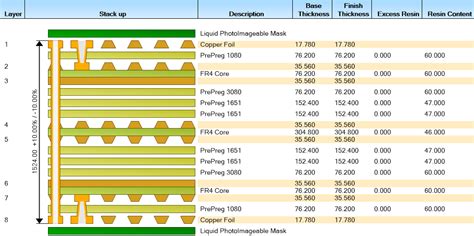
RAYPCB Stackup Table
To provide a clear overview of RAYPCB’s updated standard stackup, we have created a table that summarizes the key specifications:
| Layer | Material | Thickness (mm) | Copper Weight (oz) |
|---|---|---|---|
| Top Solder Mask | LPI | 0.025 | – |
| Top Copper | Copper | 0.035 | 1 |
| Prepreg | 2116 | 0.2 | – |
| Inner Copper 1 | Copper | 0.018 | 0.5 |
| Core | FR-4 | 0.2 | – |
| Inner Copper 2 | Copper | 0.018 | 0.5 |
| Prepreg | 2116 | 0.2 | – |
| Bottom Copper | Copper | 0.035 | 1 |
| Bottom Solder Mask | LPI | 0.025 | – |
Note: The above table represents a simplified 4-layer stackup. RAYPCB’s updated standard stackup supports up to 16 layers with customizable materials and thicknesses based on specific project requirements.
Frequently Asked Questions (FAQ)
-
Q: What is the maximum number of layers supported by RAYPCB’s updated standard stackup?
A: RAYPCB’s updated standard stackup supports up to 16 layers, providing designers with ample flexibility for complex PCB designs. -
Q: Does RAYPCB offer impedance control in their standard stackup?
A: Yes, RAYPCB’s updated standard stackup incorporates impedance control techniques, including controlled impedance and differential impedance, to ensure consistent signal propagation and integrity. -
Q: What advanced materials are used in RAYPCB’s updated standard stackup?
A: RAYPCB’s updated standard stackup utilizes advanced materials such as High-Tg FR-4, Isola TerraGreen, and Rogers RO4000-series laminates to enhance the performance and reliability of PCBs. -
Q: Are blind and buried vias supported in RAYPCB’s standard stackup?
A: Yes, RAYPCB’s updated standard stackup supports the use of blind and buried vias, enabling designers to create denser and more efficient PCB layouts. -
Q: How does RAYPCB ensure consistent layer thicknesses in their standard stackup?
A: RAYPCB implements controlled thickness for all layers through precise material selection, lamination process control, and advanced manufacturing techniques, ensuring that PCBs meet the specified dimensions and tolerances.
Conclusion
RAYPCB’s updated standard stackup for multi-layer PCBs represents a significant advancement in PCB design and manufacturing. By incorporating increased layer counts, impedance control, advanced materials, blind/buried vias, and controlled thickness, RAYPCB enables designers to create high-performance, reliable, and cost-effective PCBs.
The benefits of RAYPCB’s updated stackup extend beyond technical specifications. With a standardized approach and streamlined manufacturing process, RAYPCB can deliver high-quality PCBs faster, helping customers reduce time-to-market and stay competitive in the rapidly evolving electronics industry.
As PCB complexity continues to increase, having a well-defined and adaptable standard stackup becomes crucial. RAYPCB’s commitment to continuous improvement and customer satisfaction positions them as a trusted partner for PCB design and manufacturing.
If you have any further questions or require assistance with your PCB project, please don’t hesitate to contact RAYPCB’s technical support team. They will be happy to provide you with expert guidance and help you leverage the full potential of their updated standard stackup.
Leave a Reply