RF & Microwave Blog
-
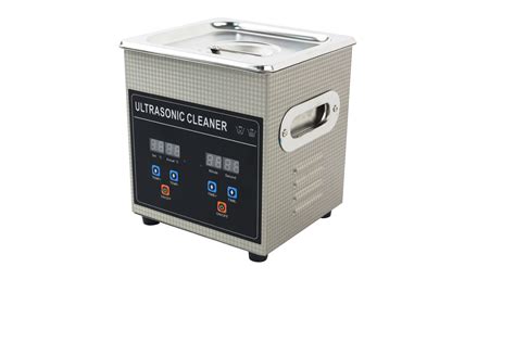
 Read more: How to Use an Ultrasonic Cleaner to Restore Electronics and PCBs
Introduction to Ultrasonic Cleaners An ultrasonic cleaner is a powerful tool that uses high-frequency sound waves to clean and restore various objects, including electronics and printed circuit boards (PCBs). The cleaning process involves submerging the item in a cleaning solution and subjecting it to ultrasonic vibrations, which create microscopic bubbles […]
-
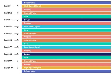 Read more: Check Now RAYPCB Updates its Standard Stackup for Multi layer PCBs
Understanding PCB Stackups A PCB stackup refers to the arrangement of layers within a printed circuit board, including the copper layers, insulating layers, and other materials used in the construction of the board. The stackup plays a critical role in determining the electrical, mechanical, and thermal properties of the PCB, […]
-
Why is controlled impedance so important
Posted by
–
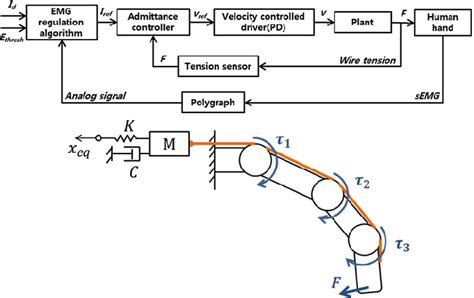 Read more: Why is controlled impedance so important
What is Controlled Impedance? Controlled impedance refers to the precise management of the impedance of a transmission line, such as a printed circuit board (PCB) trace or cable, to match the characteristic impedance of the system. Impedance is the measure of opposition to the flow of alternating current (AC) in […]
-
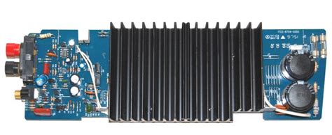 Read more: multi layer PCB design and ground free area in Altium
Introduction to Multi-Layer PCB Design Multi-layer printed circuit boards (PCBs) are essential for modern electronics that require high density interconnects and complex circuitry. Compared to single or double-layer boards, multi-layer PCBs offer several advantages: Increased circuit density and miniaturization Better signal integrity and reduced crosstalk Improved power distribution and thermal […]
-
PCB manufacturer in Thailand
Posted by
–
 Read more: PCB manufacturer in Thailand
Introduction to PCB Manufacturing in Thailand Thailand has emerged as a major hub for electronics manufacturing in Southeast Asia, including the production of printed circuit boards (PCBs). The country’s strategic location, skilled workforce, and supportive government policies have attracted numerous international companies to establish their PCB manufacturing facilities in Thailand. […]
-
Do you know the deal with square traces on PCBs
Posted by
–
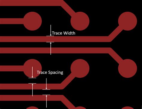 Read more: Do you know the deal with square traces on PCBs
What are square traces on a PCB? Square traces, also known as rectangular traces, refer to the shape of the copper conductors used to route signals on a printed circuit board (PCB). Unlike traditional rounded traces, square traces have 90-degree angles and a rectangular cross-section. Square traces offer several advantages […]
-
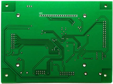 Read more: Analysis and Control of crosstalk in high speed PCB design
Introduction to Crosstalk in PCBs Crosstalk is a major concern in high-speed printed circuit board (PCB) designs. As signal speeds and component densities increase, the coupling of electromagnetic energy between adjacent traces, known as crosstalk, becomes more pronounced. Crosstalk can lead to signal integrity issues, such as overshoots, undershoots, ringing, […]
-
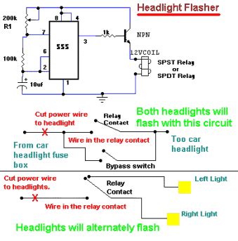 Read more: Shanghai Excelle not closed headlight reminder buzzer circuit diagram
Introduction to Headlight Reminder Circuits In modern automobiles, safety features have become increasingly important. One such feature is the headlight reminder circuit, which alerts the driver if they have left their headlights on after turning off the vehicle. This simple yet effective system can help prevent battery drain and improve […]
-
Advanced Circuits Terms and Conditions
Posted by
–
 Read more: Advanced Circuits Terms and Conditions
Overview of Advanced Circuits Terms & Conditions Advanced Circuits is committed to providing high-quality printed circuit board (PCB) manufacturing services to our customers. By placing an order with Advanced Circuits, you agree to be bound by the following terms and conditions. Please read these terms carefully before submitting your order. […]
-
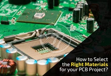 Read more: How to choose the right PCB material in your electronic project
Understanding PCB Materials PCB materials, also known as substrates, are the foundation of a printed circuit board. They provide mechanical support and electrical insulation for the copper traces and components mounted on the board. The most common PCB materials are: FR-4 (Flame Retardant 4) High-Frequency Laminates Flexible PCB Materials Metal […]
Recent Posts
- How to Select Material for Your PCBs from Cost and Reliability Considerations
- Problems of EMC Technology Application in PCB Design of Electronic Devices and the Strategies
- Fabrication Technology on Flex-Rigid PCB Window
- Problems of High-Frequency and High-Speed Multilayer PCB Fabrication and Their Solutions
- Key Difficulties and Tips for Backplane PCB Fabrication