RF & Microwave Blog
-
Read more: An Introduction of Organic Solderability Preservative OSP by RAYPCB
What is Organic Solderability Preservative (OSP)? Organic Solderability Preservative (OSP) is a chemical finish applied to printed circuit boards (PCBs) to protect exposed copper from oxidation and ensure good solderability. OSP provides a protective layer on the copper surface, preventing it from reacting with the environment and maintaining its solderability […]
-
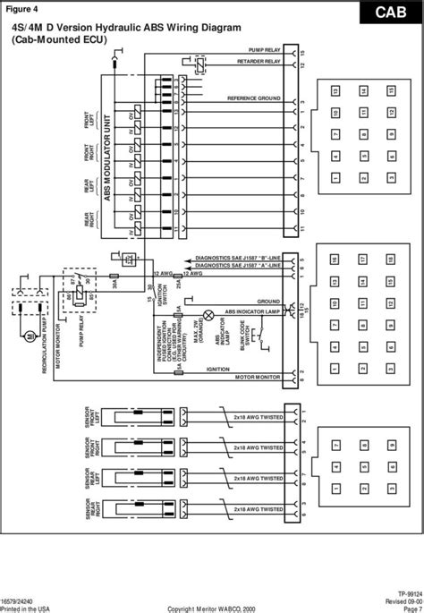
Anti lock braking system schematics
Posted by
–
 Read more: Anti lock braking system schematics
Introduction to ABS Schematics Anti-lock Braking System (ABS) is a critical safety feature in modern vehicles that prevents the wheels from locking up during sudden or hard braking. This system allows the driver to maintain steering control and reduces the stopping distance, especially on slippery roads. Understanding the schematics of […]
-
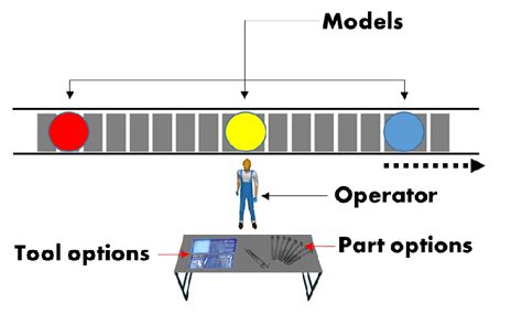
Mixed Assembly Advantages
Posted by
–
 Read more: Mixed Assembly Advantages
What is Mixed Assembly? Mixed assembly refers to the process of combining different manufacturing methods to produce a single product. This can include using a mix of automated machines and manual labor, or combining different automated processes such as CNC machining, 3D printing, and injection molding. The goal of mixed […]
-
What Is Copper Clad Laminate CCL
Posted by
–
 Read more: What Is Copper Clad Laminate CCL
Composition and Structure of Copper Clad Laminate Copper Foil Layer The copper foil layer in CCL is typically made of high-purity, electrodeposited copper. The thickness of the copper foil can vary depending on the application and the desired electrical properties of the PCB. Common copper foil thicknesses include: Copper Foil […]
-
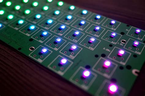
What Is LED PCB
Posted by
–
 Read more: What Is LED PCB
Introduction to LED PCB An LED PCB, or Light Emitting Diode Printed Circuit Board, is a specialized type of circuit board designed to efficiently power and control LED lights. LEDs have gained immense popularity in recent years due to their energy efficiency, long lifespan, and versatility in various applications. LED […]
-
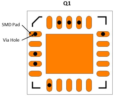
What Is Via in Pad
Posted by
–
 Read more: What Is Via in Pad
Introduction to Via-in-Pad Technology Via-in-Pad (VIP) is a technology used in printed circuit board (PCB) design and manufacturing that allows for the placement of vias directly within the surface mount pads of components. This innovative technique has gained popularity in recent years due to its numerous benefits, including improved signal […]
-
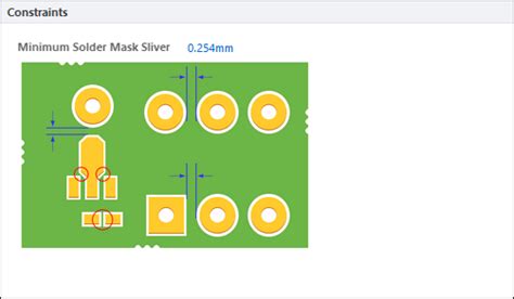 Read more: What Is The Difference Between Solder Mask And Solder Paste
Introduction In the world of electronics manufacturing, two terms that often cause confusion are Solder mask and solder paste. While they may sound similar, they serve very different purposes in the printed circuit board (PCB) assembly process. Understanding the difference between solder mask and solder paste is crucial for anyone […]
-
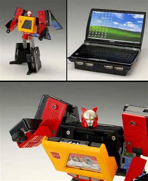
Laptops transformers the pros and cons of choice
Posted by
–
 Read more: Laptops transformers the pros and cons of choice
What are Laptop Transformers? Laptop transformers, also known as 2-in-1 laptops or convertible laptops, are devices that can function both as a laptop and a tablet. They feature a unique design that enables the screen to rotate, fold, or detach from the keyboard, allowing users to switch between various modes, […]
-
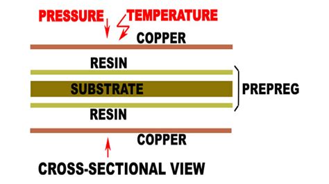
 Read more: An Introduction to The PCB Lamination Process by RAYPCB
What is PCB Lamination? PCB lamination is the process of bonding multiple layers of PCB materials together to create a single, solid board. The process involves applying heat and pressure to the layers, which causes the resin in the prepreg material to flow and bond the layers together. The resulting […]
-
Mentor Graphics Launches New Xpedition Platform to Optimize Advanced PCB Systems Design Productivity
Posted by
–
 Read more: Mentor Graphics Launches New Xpedition Platform to Optimize Advanced PCB Systems Design Productivity
Introduction to the Xpedition Platform Mentor Graphics, a leading provider of electronic design automation (EDA) solutions, has announced the launch of its new Xpedition Platform, designed to optimize the productivity of advanced printed circuit board (PCB) systems design. The Xpedition Platform is a comprehensive suite of tools that streamlines the […]
Recent Posts
- How to Select Material for Your PCBs from Cost and Reliability Considerations
- Problems of EMC Technology Application in PCB Design of Electronic Devices and the Strategies
- Fabrication Technology on Flex-Rigid PCB Window
- Problems of High-Frequency and High-Speed Multilayer PCB Fabrication and Their Solutions
- Key Difficulties and Tips for Backplane PCB Fabrication