What is PCB Wire Strain Relief and Why is it Important?
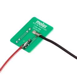
PCB wire strain relief refers to methods and techniques used to prevent mechanical stress and strain on wires and cables connected to a printed circuit board (PCB). When wires are soldered directly to a PCB without any strain relief, any pulling, twisting, or vibration of the wires can damage the solder joints or even rip the pads right off the board. This can lead to loose connections, intermittent failures, and complete loss of functionality.
Proper PCB wire strain relief is critical for ensuring the reliability and longevity of electronic devices, especially those subjected to movement, impacts, or harsh environments. By securing the wires and absorbing any mechanical forces, strain relief methods help maintain the integrity of electrical connections and prevent costly failures.
Common Methods for PCB Wire Strain Relief
There are several methods commonly used to provide strain relief for wires connected to a PCB. Each has its own advantages and is suited for different applications. Some of the most popular PCB wire strain relief techniques include:
Cable Ties or Zip Ties
One of the simplest and most economical methods for strain relief is using cable ties or zip ties to bundle and secure wires to the PCB or enclosure. The ties can be threaded through holes in the board or anchored to nearby structures. When tightened, they grip the wires and take up any slack, preventing the wires from pulling on the solder joints.
Advantages:
– Inexpensive and readily available
– Quick and easy to install
– Can be used with various wire gauges and bundle sizes
Disadvantages:
– Limited holding strength, especially for heavy or stiff wires
– Can loosen over time due to vibration or temperature changes
– May not provide adequate strain relief for high-reliability applications
Strain Relief Connectors
Strain relief connectors, also known as cord grips or cable glands, are specialized fittings that clamp around the wire insulation and screw into a threaded hole in the PCB or enclosure. They provide a strong mechanical connection and transfer any pulling forces from the wire to the connector body and mounting surface.
Advantages:
– Robust and secure strain relief for heavy-duty applications
– Can accommodate various wire gauges and insulation materials
– Provides environmental sealing to keep out moisture and debris
Disadvantages:
– More expensive than simple ties or clamps
– Requires a threaded hole in the PCB or enclosure
– May not be suitable for very thin or fragile wires
Adhesive Cable Clamps
Adhesive-backed cable clamps are plastic or metal clips that stick to the PCB or enclosure and hold the wires in place. They come in various sizes and can be used to route wires across the board or provide anchor points for strain relief. The adhesive is usually a strong pressure-sensitive acrylic that bonds well to most surfaces.
Advantages:
– Easy to apply, even on irregular surfaces
– Low profile and takes up minimal space
– Can be repositioned if needed before the adhesive fully sets
Disadvantages:
– Adhesive may weaken over time, especially in high temperatures or humidity
– Not suitable for heavy wires or high-vibration environments
– Requires a clean, flat surface for proper bonding
Wire Tie Mounts
Wire tie mounts are small plastic or metal anchors that are soldered or screwed to the PCB and provide attachment points for cable ties. They allow you to route and secure wires along the board without the need for drilled holes. Some designs have multiple tie points for bundling wires in parallel.
Advantages:
– Provides organized wire routing and strain relief
– Easy to install using existing hardware or solder points
– Compatible with standard cable ties
Disadvantages:
– Adds extra components and assembly steps
– Limited holding strength compared to connectors or clamps
– May obstruct other components or test points on the PCB
Rubber Grommets
Rubber grommets are soft, flexible rings that fit into holes in the PCB or enclosure and provide a protected passage for wires. They cushion the wires and absorb vibrations, preventing chafing and abrasion of the insulation. Grommets can be used alone or in combination with cable ties for added strain relief.
Advantages:
– Protects wires from sharp edges and vibration damage
– Can be easily installed in drilled or punched holes
– Provides some environmental sealing against dust and moisture
Disadvantages:
– Requires precise hole sizes for proper fit
– May not grip the wires tightly enough for high-stress applications
– Can be damaged or dislodged by repeated insertion and removal of wires

Factors to Consider When Choosing a PCB Wire Strain Relief Method
With so many strain relief options available, it can be challenging to select the best one for your specific application. Here are some key factors to consider when evaluating PCB wire strain relief methods:
Mechanical Strength
The strain relief method must be strong enough to withstand the expected mechanical forces, such as pulling, twisting, and vibration, without damaging the wires or PCB. Consider the weight and stiffness of the wires, as well as any shock or acceleration loads the device may experience.
Environmental Factors
Different strain relief methods offer varying levels of protection against environmental factors like moisture, dust, chemicals, and extreme temperatures. Choose a method that can withstand the anticipated operating conditions and provide any necessary sealing or insulation.
Space Constraints
PCB real estate is often limited, so the strain relief method should be compact and unobtrusive. Consider the size and orientation of the components, connectors, and mounting holes, and choose a strain relief solution that fits within those constraints.
Ease of Assembly
The strain relief method should be easy to install and compatible with your existing manufacturing processes. Some methods require special tools or additional assembly steps, which can increase production time and costs.
Cost
Like any component, the cost of the strain relief method must be balanced against its performance and reliability benefits. Consider the total cost of materials, labor, and any necessary tooling or equipment changes.
Compatibility
Ensure that the chosen strain relief method is compatible with the wire gauges, insulation materials, and connector types used in your application. Some methods may not work well with very thin or thick wires or may require special adapters for certain connector styles.

Best Practices for Implementing PCB Wire Strain Relief
Proper implementation is key to achieving effective PCB wire strain relief. Here are some best practices to follow when designing and assembling your strain relief system:
Plan Ahead
Incorporate strain relief considerations early in the PCB design process. This allows you to optimize component placement, routing, and mounting holes for the chosen strain relief method. Retrofitting strain relief to an existing design can be challenging and may compromise performance.
Use Appropriate Materials
Select strain relief components that are made from durable, high-quality materials compatible with your wires and PCB. Avoid using materials that may degrade or become brittle over time, such as low-grade plastics or adhesives.
Provide Adequate Slack
Leave enough slack in the wires between the strain relief point and the solder joint to allow for some movement and flexibility. This reduces stress on the joint and prevents the wire from being pulled taut, which could cause damage.
Secure the Wires
Ensure that the wires are securely fastened within the strain relief device, with no slipping or loosening over time. Follow the manufacturer’s instructions for tightening cable ties, screws, or clamps to the proper torque.
Avoid Sharp Bends
Route the wires in gentle curves rather than sharp bends, which can stress the insulation and cause premature failure. Use strain relief methods that provide smooth, gradual transitions and avoid pinching or crimping the wires.
Test and Inspect
After assembly, thoroughly test the strain relief system to ensure it performs as intended. Apply controlled mechanical forces to the wires and check for any signs of slipping, damage, or disconnection. Regularly inspect the strain relief components and wires during use to identify any wear or deterioration.

Strain Relief Methods Comparison Table
| Method | Strength | Environmental Protection | Space Efficiency | Ease of Assembly | Cost |
|---|---|---|---|---|---|
| Cable Ties | Low to Medium | Low | High | Easy | Low |
| Strain Relief Connectors | High | High | Medium | Moderate | High |
| Adhesive Cable Clamps | Low to Medium | Low to Medium | High | Easy | Low to Medium |
| Wire Tie Mounts | Medium | Low to Medium | Medium | Moderate | Medium |
| Rubber Grommets | Low to Medium | Medium | Medium | Easy | Low |
FAQ
1. What is the most secure method for PCB wire strain relief?
Strain relief connectors, also known as cord grips or cable glands, offer the highest level of security and mechanical strength. They provide a robust connection that transfers pulling forces away from the delicate solder joints and onto the connector body and mounting surface.
2. Can I use multiple strain relief methods together?
Yes, combining different strain relief methods can provide added protection and redundancy. For example, you can use rubber grommets to protect wires from sharp edges, then secure them with cable ties or clamps for additional strain relief.
3. How much slack should I leave in the wires for strain relief?
The appropriate amount of slack depends on the wire gauge, insulation material, and expected range of motion. As a general rule, leave enough slack to allow the wires to flex and move slightly without putting tension on the solder joints. Typically, a few millimeters to a centimeter of slack is sufficient.
4. Can I add strain relief to an existing PCB design?
While it’s best to incorporate strain relief early in the design process, it is possible to retrofit strain relief to an existing PCB. However, you may need to modify the board layout, drill new mounting holes, or use adhesive-backed solutions that don’t require physical changes to the PCB.
5. How often should I inspect the strain relief components?
Regular inspections are important to ensure the continued effectiveness of your strain relief system. The frequency of inspections depends on the application and environmental conditions, but a good starting point is to check the strain relief components and wires at least once every few months or after any significant mechanical events, such as drops or impacts.
Conclusion
Effective PCB wire strain relief is essential for maintaining the reliability and longevity of electronic devices. By understanding the various strain relief methods available and considering factors like mechanical strength, environmental protection, and ease of assembly, you can select the best solution for your specific application.
Remember to follow best practices during implementation, such as planning ahead, using appropriate materials, and testing thoroughly. Regular inspections and maintenance will help ensure your strain relief system continues to perform as intended over the life of the product.
With proper PCB wire strain relief in place, you can reduce the risk of costly failures, improve product quality, and enhance customer satisfaction.
Leave a Reply