What is PCB Strain Relief and Why is it Important?
Printed Circuit Board (PCB) strain relief is a method of securing and protecting the wires or cables that connect to a PCB. The purpose of strain relief is to prevent the wires from being pulled, twisted, or bent in a way that could damage the electrical connections or the PCB itself.
When wires are connected to a PCB without proper strain relief, any movement or tension on the wires can cause them to tug on the solder joints or copper traces. Over time, this repeated stress can lead to broken connections, damaged components, or even complete failure of the PCB assembly.
Implementing effective PCB strain relief is crucial for ensuring the long-term reliability and durability of electronic devices. It is especially important in applications where the PCB may be subject to vibration, impact, or frequent handling.
Common Methods of PCB Strain Relief
There are several common methods used to provide strain relief for wires connected to a PCB. The choice of method depends on factors such as the size and type of wires, the available space on the PCB, and the expected level of stress on the connections.
Cable Ties
One of the simplest forms of strain relief is to use cable ties to bundle and secure the wires to the PCB or chassis. Cable ties can be threaded through holes in the PCB or wrapped around mounting posts. They provide a quick and inexpensive way to keep wires organized and prevent them from pulling on the solder joints.
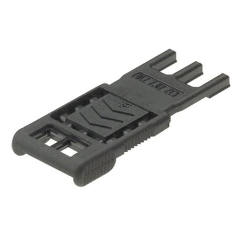
Strain Relief Connectors
Strain relief connectors are specialized components that are designed to grip and secure wires as they enter or exit a PCB. These connectors typically have a plastic or metal housing with a clamping mechanism that holds the wires in place. Some common types of strain relief connectors include:
- Barrel connectors
- Grommet connectors
- Brush strip connectors
- D-sub connectors
Strain relief connectors provide a neat and professional appearance while also offering robust protection against wire strain.
Adhesive Strain Relief
Adhesive strain relief involves using a strong, flexible adhesive to bond the wires to the PCB or enclosure. This method is often used in applications where space is limited or where the wires need to be routed in a specific way.
One common type of adhesive strain relief is hot glue. Hot glue guns can be used to apply a bead of molten adhesive around the base of the wires where they connect to the PCB. As the glue cools and hardens, it forms a strong bond that resists pulling and bending forces.
Another option is to use specialized adhesive products such as 3M Dual Lock or Hook and Loop fasteners. These products have a pressure-sensitive adhesive backing that can be applied to both the wires and the PCB, allowing them to be securely fastened together.
Mechanical Strain Relief
Mechanical strain relief involves using physical structures or devices to support and secure the wires. Some examples of mechanical strain relief include:
- Mounting clips or brackets that hold the wires in place
- Strain relief glands or bushings that fit around the wires and screw into the PCB or chassis
- 3D printed structures that are custom-designed to fit the specific wire arrangement
Mechanical strain relief can be very effective at preventing wire damage, but it often requires more space and additional hardware compared to other methods.

Factors to Consider When Choosing a Strain Relief Method
When selecting a strain relief method for a PCB design, there are several key factors to consider:
Wire Gauge and Type
The size and type of wires being used will influence the choice of strain relief method. Thicker wires may require stronger clamping force or larger connectors, while thinner wires may be more prone to damage from sharp bends or pinching.
The insulation material of the wires is also important. Some materials such as PVC are more flexible and forgiving, while others like Teflon are stiffer and more prone to cracking if bent too sharply.
Available Space
The amount of space available on the PCB and in the surrounding enclosure will limit the options for strain relief. In tight spaces, adhesive or small connector-based methods may be preferable over bulky mechanical solutions.
It’s important to consider not just the space taken up by the strain relief itself, but also the clearance needed for installing and servicing the wires. There should be enough room for the wires to be safely routed and for technicians to access the connections if needed.
Expected Stress Level
The expected level of stress on the wires will determine how robust the strain relief needs to be. In applications where the PCB will be subject to frequent movement, vibration, or impact, a stronger mechanical solution may be necessary.
For example, in automotive or aerospace applications, the strain relief may need to withstand high levels of shock and vibration. In these cases, specialized connectors or mounting hardware may be required to ensure the wires remain securely attached.
Cost and Manufacturing Considerations
The cost and complexity of the strain relief solution should be balanced against the overall cost and manufacturing process for the PCB assembly.
Simple methods like cable ties or adhesive are inexpensive and easy to implement, but may not provide adequate protection in high-stress environments. More sophisticated solutions like custom strain relief connectors offer better performance but come with higher costs and longer lead times.
It’s important to consider the strain relief design early in the PCB development process, as it can impact the layout and component placement on the board. Involving the manufacturing team in the design process can help ensure the strain relief solution is compatible with the assembly process and does not add unnecessary cost or complexity.

Best Practices for PCB Strain Relief Design
To ensure effective and reliable strain relief in a PCB design, follow these best practices:
-
Plan for strain relief early in the design process. Don’t treat strain relief as an afterthought – consider it as an integral part of the PCB design from the beginning.
-
Use the appropriate gauge and type of wire. Select wires that are rated for the expected current and voltage levels, and choose insulation materials that are compatible with the strain relief method being used.
-
Provide adequate clearance for wires and connectors. Make sure there is enough space around the strain relief components for the wires to be routed safely and for technicians to access the connections if needed.
-
Use a combination of strain relief methods. In some cases, a single strain relief method may not be sufficient. Consider using a combination of methods, such as a connector with a cable tie backup, to provide redundant protection.
-
Test the strain relief design. Before finalizing the PCB design, create prototypes or mockups to test the effectiveness of the strain relief solution. Apply realistic stress levels and observe how the wires and connections hold up over time.
-
Document the strain relief requirements. Include clear instructions and specifications for the strain relief components in the PCB documentation, including the wire gauge, insulation type, and any special installation or maintenance requirements.
By following these best practices and carefully considering the specific requirements of the application, designers can create PCB strain relief solutions that provide reliable protection for wires and ensure the long-term integrity of the electronic assembly.

PCB Strain Relief Design Comparison
To help designers choose the best strain relief method for their application, here is a comparison table of the common methods:
| Method | Pros | Cons |
|---|---|---|
| Cable Ties | – Inexpensive – Easy to install – Versatile |
– Limited strength – Can loosen over time – May not meet aesthetic requirements |
| Strain Relief Connectors | – Robust clamping force – Professional appearance – Designed for wire management |
– Higher cost – Requires specific connectors – May not fit in tight spaces |
| Adhesive Strain Relief | – Low cost – Minimal space requirements – Customizable |
– Limited strength – Can degrade over time – May not be suitable for high-stress applications |
| Mechanical Strain Relief | – High strength – Can be customized for specific wire arrangements – Durable |
– Higher cost – Requires additional hardware – May not fit in tight spaces |
Frequently Asked Questions (FAQ)
-
Q: How do I know which strain relief method is best for my PCB design?
A: The best strain relief method depends on factors such as the wire gauge and type, available space, expected stress level, and cost constraints. Consider the pros and cons of each method and choose the one that best meets your specific requirements. -
Q: Can I use multiple strain relief methods on the same PCB?
A: Yes, in some cases it may be beneficial to use a combination of strain relief methods to provide redundant protection. For example, you could use a strain relief connector with a cable tie backup to ensure the wires remain secure even if one method fails. -
Q: How much space do I need to allocate for strain relief components?
A: The space required for strain relief components varies depending on the method being used. Cable ties and adhesive methods typically require minimal space, while connectors and mechanical solutions may need more clearance. Be sure to consider not just the space taken up by the components themselves, but also the room needed for wire routing and maintenance access. -
Q: What if I don’t have room for dedicated strain relief components on my PCB?
A: If space is limited, consider using adhesive strain relief methods or small strain relief connectors that can be integrated into the existing PCB layout. You can also explore creative solutions like 3D printed strain relief structures that are custom-designed to fit your specific wire arrangement. -
Q: How can I test the effectiveness of my strain relief design?
A: To test your strain relief design, create prototypes or mockups of the PCB assembly and apply realistic stress levels to the wires. Observe how the connections hold up over time and make adjustments as needed. You can also conduct accelerated life testing by subjecting the assembly to high levels of vibration, temperature cycling, or other environmental stresses to simulate long-term use.
By understanding the different PCB strain relief methods and following best practices for design and testing, you can create robust and reliable electronic assemblies that stand up to the demands of real-world use.
Leave a Reply