Understanding the Polygon Pour Issue in Altium Designer
When designing rigid-flex PCBs in Altium Designer, a common issue arises with polygon pour breaks along the split lines between the rigid and flexible sections. This problem can lead to inconsistencies in the copper distribution, potentially affecting the electrical performance and manufacturability of the board. In this article, we will dive deep into the causes of this issue and explore various solutions to ensure a seamless polygon pour across rigid-flex split lines.
What Causes Polygon Pour Breaks on Rigid Flex Split Lines?
Polygon pour breaks on rigid-flex split lines can occur due to several factors:
- Incorrect layer stack definition
- Improper split line placement
- Incompatible polygon pour settings
- Insufficient clearance between split lines and components
Let’s examine each of these factors in detail.
Incorrect Layer Stack Definition
A properly defined layer stack is crucial for achieving a consistent polygon pour across rigid-flex split lines. When setting up the layer stack in Altium Designer, consider the following:
- Ensure that the layer stack accurately represents the structure of your rigid-flex PCB, including the correct number of layers and their respective thicknesses.
- Define the appropriate layer types, such as signal, plane, or dielectric, for each layer in the stack.
- Specify the correct material properties for each layer, including the dielectric constant and loss tangent.
Here’s an example of a well-defined layer stack for a 4-layer rigid-flex PCB:
| Layer | Type | Material | Thickness (mm) |
|---|---|---|---|
| Top | Signal | Copper | 0.035 |
| L2 | Plane | Copper | 0.035 |
| L3 | Plane | Copper | 0.035 |
| Bottom | Signal | Copper | 0.035 |
| Core | Dielectric | FR-4 | 0.2 |
| Flex | Dielectric | Polyimide | 0.05 |
Improper Split Line Placement
The placement of split lines between rigid and flexible sections plays a significant role in maintaining a continuous polygon pour. When placing split lines, consider the following guidelines:
- Place split lines at the boundaries between rigid and flexible sections, ensuring that they accurately represent the mechanical transitions of the PCB.
- Avoid placing split lines too close to components or other design features, as this can lead to insufficient clearance and potential manufacturing issues.
- Ensure that split lines are placed on all relevant layers, including signal and plane layers, to maintain consistency across the layer stack.
Here’s an illustration of proper split line placement in a rigid-flex PCB:
    Rigid Section    |    Flexible Section
                     |
       +-----------+ |
       |           | |
       |           | |
       |           | |
       +-----------+ |
                     |
  Split Line --->    |
Incompatible Polygon Pour Settings
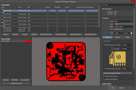
Polygon pour settings in Altium Designer can greatly impact the continuity of copper distribution across rigid-flex split lines. To ensure a seamless polygon pour, consider the following settings:
- Remove Dead Copper: Enable the “Remove Dead Copper” option in the polygon pour properties to eliminate isolated copper areas that may cause discontinuities.
- Thermal Relief Settings: Configure the thermal relief settings to ensure proper connection between the polygon pour and component pads, while allowing for sufficient heat dissipation during soldering.
- Polygon Connect Style: Choose an appropriate polygon connect style, such as “Direct Connect” or “Relief Connect,” based on your design requirements and manufacturing capabilities.
Here’s a table comparing the polygon connect styles:
| Connect Style | Description | Advantages | Disadvantages |
|---|---|---|---|
| Direct Connect | Polygon directly connects to the pad | Minimal impedance mismatch | Difficult to solder |
| Relief Connect | Thermal reliefs are added between polygon and pad | Easier to solder | Slightly higher impedance |
Insufficient Clearance Between Split Lines and Components
Maintaining adequate clearance between split lines and components is essential for preventing polygon pour breaks. When placing components near split lines, consider the following:
- Adhere to the minimum clearance requirements specified by your PCB manufacturer to ensure proper fabrication and assembly.
- Use the clearance constraint tools in Altium Designer to define and enforce clearance rules between split lines and components.
- Perform a design rule check (DRC) to identify any clearance violations and resolve them before finalizing your design.
Here’s an example of clearance constraints in Altium Designer:
Clearance Constraint: Split Line to Component Pad
Scope: All
Minimum Clearance: 0.2 mm
Resolving Polygon Pour Breaks on Rigid Flex Split Lines
Now that we understand the causes of polygon pour breaks on rigid-flex split lines, let’s explore some solutions to resolve this issue.
Solution 1: Redefining the Layer Stack
If you suspect that an incorrect layer stack definition is causing the polygon pour breaks, follow these steps to redefine the layer stack:
- Open the Layer Stack Manager in Altium Designer.
- Verify that the layer stack accurately represents your rigid-flex PCB structure, including the correct number of layers, layer types, and thicknesses.
- Ensure that the appropriate material properties are assigned to each layer.
- Save the updated layer stack and reapply it to your PCB design.
Solution 2: Adjusting Split Line Placement
Improper split line placement can lead to polygon pour breaks. To resolve this issue:
- Review the placement of split lines in your design, ensuring that they accurately represent the transitions between rigid and flexible sections.
- Adjust split lines to maintain sufficient clearance from components and other design features.
- Verify that split lines are placed on all relevant layers, including signal and plane layers.
- Perform a design rule check to identify and resolve any clearance violations.
Solution 3: Optimizing Polygon Pour Settings
Incompatible polygon pour settings can cause discontinuities in the copper distribution. To optimize your polygon pour settings:
- Access the polygon pour properties in Altium Designer.
- Enable the “Remove Dead Copper” option to eliminate isolated copper areas.
- Configure the thermal relief settings to ensure proper connection between the polygon pour and component pads, while allowing for sufficient heat dissipation during soldering.
- Choose an appropriate polygon connect style based on your design requirements and manufacturing capabilities.
Solution 4: Ensuring Adequate Clearance
Insufficient clearance between split lines and components can lead to polygon pour breaks. To ensure adequate clearance:
- Review your PCB manufacturer’s minimum clearance requirements and ensure that your design adheres to these guidelines.
- Use the clearance constraint tools in Altium Designer to define and enforce clearance rules between split lines and components.
- Perform a design rule check to identify and resolve any clearance violations.

Frequently Asked Questions (FAQ)
-
Q: Can I use the same polygon pour settings for both rigid and flexible sections?
A: While it’s possible to use the same polygon pour settings for both rigid and flexible sections, it’s often recommended to adjust the settings based on the specific requirements of each section. For example, flexible sections may require a different polygon connect style or thermal relief settings compared to rigid sections. -
Q: How can I ensure that my rigid-flex PCB is manufacturable?
A: To ensure the manufacturability of your rigid-flex PCB, follow these guidelines: - Adhere to your PCB manufacturer’s design rules and requirements.
- Maintain adequate clearance between components, traces, and split lines.
- Use appropriate materials and layer stack configuration for your application.
-
Perform thorough design rule checks and address any violations.
-
Q: What should I do if I still encounter polygon pour breaks after applying the solutions mentioned in this article?
A: If you continue to experience polygon pour breaks after applying the solutions, consider the following additional steps: - Verify that your design is free of any copper or component overlaps that may interfere with the polygon pour.
- Ensure that your polygon pour settings are consistent across all layers and sections of the PCB.
-
Consult with your PCB manufacturer for specific guidance on resolving polygon pour breaks in your design.
-
Q: Can I use different polygon pour settings for different layers in my rigid-flex PCB?
A: Yes, you can define different polygon pour settings for each layer in your rigid-flex PCB. This allows you to optimize the copper distribution based on the specific requirements of each layer, such as signal integrity, power delivery, or shielding. -
Q: How do I ensure proper grounding in my rigid-flex PCB design?
A: To ensure proper grounding in your rigid-flex PCB design: - Use dedicated ground planes to provide a low-impedance return path for signals.
- Connect ground planes across rigid and flexible sections using appropriate via stitching and copper pours.
- Maintain continuous ground connections throughout the layer stack, avoiding any breaks or discontinuities.
- Use ground stitching vias along split lines to provide additional grounding points and minimize potential EMI issues.

Conclusion
Polygon pour breaks on rigid-flex split lines can be a frustrating issue when designing PCBs in Altium Designer. By understanding the causes of this problem, such as incorrect layer stack definition, improper split line placement, incompatible polygon pour settings, and insufficient clearance, you can take appropriate steps to resolve it.
Remember to:
– Define an accurate layer stack that represents your rigid-flex PCB structure.
– Place split lines accurately and maintain sufficient clearance from components.
– Optimize polygon pour settings, including removing dead copper and configuring thermal reliefs.
– Ensure adequate clearance between split lines and components using clearance constraints and design rule checks.
By following the solutions and guidelines presented in this article, you can achieve a seamless polygon pour across rigid-flex split lines, improving the electrical performance and manufacturability of your PCB design.

Leave a Reply