Introduction to Ceramic PCB
Ceramic Printed Circuit Boards (PCBs) are a specialized type of PCB that uses ceramic materials as the base substrate instead of the more common FR-4 or other organic materials. Ceramic PCBs offer unique properties that make them ideal for certain applications, particularly those that require high-temperature resistance, excellent thermal conductivity, and low dielectric loss. In this article, we will explore the world of ceramic PCBs, their manufacturing process, advantages, disadvantages, and various applications.
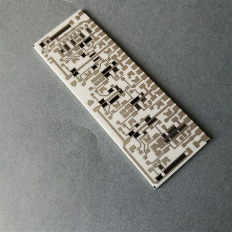
What is a Ceramic PCB?
A ceramic PCB is a printed circuit board that uses a ceramic material, such as alumina (Al2O3) or aluminum nitride (AlN), as the base substrate. The conductive traces and pads are typically made of gold, silver, or copper, which are screen-printed or plated onto the ceramic substrate. Ceramic PCBs can be single-layer or multi-layer, depending on the complexity of the circuit design.
Ceramic PCB materials
The most common ceramic materials used in PCB manufacturing are:
-
Alumina (Al2O3): Alumina is the most widely used ceramic substrate material due to its excellent electrical insulation properties, high thermal conductivity, and mechanical strength. It is also relatively inexpensive compared to other ceramic materials.
-
Aluminum Nitride (AlN): Aluminum nitride offers even higher thermal conductivity than alumina, making it an excellent choice for applications that require efficient heat dissipation. However, it is more expensive than alumina.
-
Beryllium Oxide (BeO): Beryllium oxide has the highest thermal conductivity among ceramic materials, but it is rarely used due to its toxicity and high cost.
Ceramic PCB Manufacturing Process
The manufacturing process for ceramic PCBs differs from that of traditional FR-4 PCBs. The main steps involved in ceramic PCB manufacturing are:
-
Substrate Preparation: The ceramic substrate is cut to the desired size and shape, and holes are drilled for vias and component mounting.
-
Metallization: Conductive traces and pads are applied to the ceramic substrate using screen printing or plating techniques. The most common metals used are gold, silver, and copper.
-
Firing: The metallized ceramic substrate is fired in a high-temperature furnace to bond the conductive traces and pads to the substrate.
-
Layering (for multi-layer PCBs): If a multi-layer ceramic PCB is required, additional ceramic layers with conductive traces are stacked and laminated together using a high-temperature and pressure process.
-
Component Mounting: Electronic components are soldered or attached to the ceramic PCB using various methods, such as wire bonding or surface mount technology (SMT).

Advantages of Ceramic PCBs
Ceramic PCBs offer several advantages over traditional FR-4 PCBs, including:
-
High-Temperature Resistance: Ceramic materials can withstand temperatures up to 1,000°C, making them suitable for high-temperature applications such as automotive, aerospace, and industrial equipment.
-
Excellent Thermal Conductivity: Ceramic materials, particularly aluminum nitride, have high thermal conductivity, which allows for efficient heat dissipation. This property is crucial for high-power electronic devices and applications.
-
Low Dielectric Loss: Ceramic materials have low dielectric loss, which means they have minimal signal loss and distortion at high frequencies. This property makes ceramic PCBs ideal for RF and microwave applications.
-
High Mechanical Strength: Ceramic materials are inherently strong and rigid, providing excellent mechanical stability and durability.
-
Dimensional Stability: Ceramic PCBs have a low coefficient of thermal expansion (CTE), which means they maintain their dimensions and shape even under high-temperature conditions.

Disadvantages of Ceramic PCBs
Despite their numerous advantages, ceramic PCBs also have some disadvantages, such as:
-
High Cost: Ceramic materials and the manufacturing process for ceramic PCBs are more expensive compared to traditional FR-4 PCBs. This higher cost can be a barrier for some applications.
-
Brittleness: Ceramic materials are brittle and prone to cracking or chipping if not handled carefully during the manufacturing process or in use.
-
Limited Design Flexibility: Due to the nature of ceramic materials and the manufacturing process, ceramic PCBs have limitations in terms of minimum trace width, hole size, and layer count compared to FR-4 PCBs.
-
Longer Lead Times: The manufacturing process for ceramic PCBs is more complex and time-consuming than for FR-4 PCBs, resulting in longer lead times.

Applications of Ceramic PCBs
Ceramic PCBs are used in various industries and applications that require high-temperature resistance, excellent thermal conductivity, and low dielectric loss. Some of the most common applications include:
-
Automotive Electronics: Ceramic PCBs are used in automotive applications such as engine control units, transmission control units, and exhaust gas sensors, where high-temperature resistance is crucial.
-
Aerospace and Military: Ceramic PCBs are used in aerospace and military applications, such as radar systems, satellite communications, and missile guidance systems, where reliability under extreme conditions is essential.
-
Industrial Equipment: Ceramic PCBs are used in industrial equipment, such as power inverters, motor drives, and welding equipment, where high-power handling and efficient heat dissipation are required.
-
RF and Microwave Devices: Ceramic PCBs are used in RF and microwave devices, such as antennas, filters, and amplifiers, where low dielectric loss and high-frequency performance are critical.
-
LED Lighting: Ceramic PCBs are used in high-power LED lighting applications, where efficient heat dissipation is necessary to ensure the longevity and performance of the LEDs.
Ceramic PCB vs. FR-4 PCB
The following table compares the key properties of ceramic PCBs and FR-4 PCBs:
| Property | Ceramic PCB | FR-4 PCB |
|---|---|---|
| Temperature Resistance | High | Low |
| Thermal Conductivity | High | Low |
| Dielectric Loss | Low | High |
| Mechanical Strength | High | Moderate |
| Dimensional Stability | High | Moderate |
| Cost | High | Low |
| Design Flexibility | Limited | High |
| Lead Time | Long | Short |
Future Trends in Ceramic PCB Technology
As electronic devices continue to become more advanced and compact, the demand for high-performance PCBs, including ceramic PCBs, is expected to grow. Some of the future trends in ceramic PCB technology include:
-
Improved Ceramic Materials: Researchers are developing new ceramic materials with enhanced properties, such as higher thermal conductivity, lower dielectric loss, and better mechanical strength.
-
Advancements in Manufacturing Processes: Manufacturers are continuously improving the ceramic PCB manufacturing process to achieve finer trace widths, smaller hole sizes, and higher layer counts, thus increasing design flexibility.
-
Integration with Other Technologies: Ceramic PCBs are being integrated with other advanced technologies, such as embedded components, 3D printing, and advanced packaging techniques, to create more compact and high-performance electronic devices.
-
Expansion into New Applications: As the benefits of ceramic PCBs become more widely recognized, their use is expected to expand into new applications, such as 5G communications, electric vehicles, and renewable energy systems.
FAQs
-
Q: What is the main difference between ceramic PCBs and traditional FR-4 PCBs?
A: The main difference is the base substrate material. Ceramic PCBs use ceramic materials like alumina or aluminum nitride, while FR-4 PCBs use a glass-reinforced epoxy laminate. -
Q: Are ceramic PCBs more expensive than FR-4 PCBs?
A: Yes, ceramic PCBs are generally more expensive than FR-4 PCBs due to the higher cost of ceramic materials and the more complex manufacturing process. -
Q: Can ceramic PCBs be used for all electronic applications?
A: No, ceramic PCBs are primarily used in applications that require high-temperature resistance, excellent thermal conductivity, and low dielectric loss. FR-4 PCBs are still the most common choice for general-purpose electronic applications. -
Q: What are the most common ceramic materials used in ceramic PCBs?
A: The most common ceramic materials used in PCB manufacturing are alumina (Al2O3) and aluminum nitride (AlN). -
Q: Are ceramic PCBs more environmentally friendly than FR-4 PCBs?
A: Ceramic PCBs are generally considered more environmentally friendly than FR-4 PCBs because they do not contain the same hazardous materials, such as brominated flame retardants, that are often used in FR-4 PCBs. However, the environmental impact of ceramic PCB production depends on various factors, such as the specific manufacturing processes and materials used.
Conclusion
Ceramic PCBs are a specialized type of printed circuit board that offer unique properties, such as high-temperature resistance, excellent thermal conductivity, and low dielectric loss. While they are more expensive and have some limitations compared to traditional FR-4 PCBs, ceramic PCBs are essential for applications that require reliable performance under extreme conditions. As electronic devices continue to advance, the demand for ceramic PCBs is expected to grow, driving further innovations in ceramic materials and manufacturing processes. By understanding the advantages, disadvantages, and applications of ceramic PCBs, engineers and designers can make informed decisions when selecting the most suitable PCB technology for their projects.
Leave a Reply