Understanding PCB Protection and Its Importance
Printed Circuit Boards (PCBs) are the backbone of modern electronic devices. They are used in a wide range of applications, from consumer electronics to industrial equipment and aerospace systems. However, PCBs are susceptible to various environmental factors that can cause damage and affect their performance. Therefore, it is crucial to understand the importance of PCB protection and the various methods available to safeguard these critical components.
What is PCB Protection?
PCB protection refers to the various techniques and materials used to shield printed circuit boards from environmental factors that can cause damage or affect their performance. These factors include:
- Moisture and humidity
- Dust and debris
- Extreme temperatures
- Electromagnetic interference (EMI)
- Electrostatic discharge (ESD)
- Physical damage
By implementing effective PCB protection measures, manufacturers can ensure that their products remain reliable and perform optimally throughout their lifespan.
Why is PCB Protection Important?
PCB protection is essential for several reasons:
-
Reliability: Protected PCBs are less likely to fail due to environmental factors, ensuring that the electronic device remains reliable and functional.
-
Longevity: Proper PCB protection can extend the lifespan of electronic devices by preventing damage to the components and circuitry.
-
Performance: Environmental factors can affect the performance of PCBs, leading to signal interference, data corruption, or complete device failure. PCB protection helps maintain optimal performance.
-
Cost-effectiveness: Implementing PCB protection measures during the manufacturing process is more cost-effective than repairing or replacing damaged devices later.
-
Compliance: Many industries have specific standards and regulations regarding PCB protection, such as the IPC standards for conformal coating. Meeting these requirements is essential for compliance and product acceptance.
Methods of PCB Protection
There are several methods available for protecting PCBs from environmental factors. The choice of method depends on the specific application, environmental conditions, and budget. Some common PCB protection methods include:
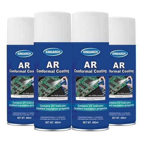
Conformal Coating
Conformal coating is a thin, protective layer applied to the surface of a PCB. It acts as a barrier against moisture, dust, and other contaminants. Conformal coatings are available in various materials, including:
- Acrylic
- Silicone
- Polyurethane
- Epoxy
- Parylene
Each material has its own advantages and disadvantages, such as ease of application, level of protection, and cost. Conformal coatings are applied using various methods, such as spraying, dipping, or brushing.
Encapsulation
Encapsulation involves completely sealing the PCB and its components in a protective material, such as epoxy or silicone. This method provides a higher level of protection than conformal coating, as it covers the entire PCB and fills any gaps or voids. Encapsulation is often used in harsh environments or applications where the PCB is exposed to significant physical stress.
Potting
Potting is similar to encapsulation but involves filling a container or “pot” with a protective material, such as epoxy or silicone, and then placing the PCB inside. This method is often used for PCBs with tall components or irregular shapes that may be difficult to coat or encapsulate directly.
Shielding
Shielding involves enclosing the PCB in a conductive material, such as metal or conductive plastic, to protect against electromagnetic interference (EMI). This method is particularly important for PCBs used in devices that are sensitive to EMI, such as medical equipment or wireless communication systems. Shielding can be achieved through various techniques, such as:
- Metal enclosures
- Conductive gaskets
- Conductive adhesives
- Shielding sprays or paints
Proper PCB Design
Effective PCB protection starts with proper PCB design. By considering the environmental factors that the PCB will be exposed to during the design phase, manufacturers can incorporate features that enhance the board’s resilience. Some design considerations for PCB protection include:
- Choosing appropriate materials for the substrate, solder mask, and components
- Incorporating adequate spacing between components and traces to minimize the risk of short circuits
- Using thicker copper traces and larger pads to improve mechanical strength
- Implementing proper grounding and shielding techniques to minimize EMI
- Selecting components with appropriate temperature ratings and packaging for the intended environment

Implementing PCB Protection in the Manufacturing Process
To ensure effective PCB protection, it is essential to integrate protection measures into the manufacturing process. This involves several key steps:
1. Cleaning
Before applying any protective coatings or encapsulants, the PCB must be thoroughly cleaned to remove any contaminants, such as flux residue, dust, or oils. Cleaning methods include:
- Solvent cleaning: Using solvents like isopropyl alcohol or specialty cleaners to dissolve and remove contaminants
- Aqueous cleaning: Using water-based solutions and detergents to clean the PCB
- Plasma cleaning: Using ionized gas to remove organic contaminants and activate the PCB surface for better coating adhesion
2. Masking
In some cases, certain areas of the PCB may need to be protected from the protective coating or encapsulant. This is achieved through masking, which involves covering these areas with a temporary material, such as tape, caps, or plugs. Masking ensures that critical components, such as connectors or test points, remain accessible and functional after the protection process.
3. Coating or Encapsulation
Once the PCB is cleaned and masked, the chosen protection method can be applied. For conformal coating, this typically involves spraying, dipping, or brushing the coating material onto the PCB surface. The coating is then cured using heat, UV light, or moisture, depending on the material.
For encapsulation or potting, the PCB is placed in a mold or container, and the encapsulant material is poured over it. The encapsulant is then cured using heat or UV light.
4. Inspection and Testing
After the protective coating or encapsulant has been applied and cured, the PCB must be inspected and tested to ensure that the protection is effective and does not interfere with the board’s functionality. This may involve:
- Visual inspection for coverage, thickness, and defects
- Electrical testing to verify that the PCB functions as intended
- Environmental testing to simulate the intended operating conditions and ensure the protection remains effective over time

Maintaining PCB Protection
Effective PCB protection does not end with the manufacturing process. It is essential to maintain the protection throughout the device’s lifespan to ensure ongoing reliability and performance. Some key considerations for maintaining PCB protection include:
Handling and Storage
PCBs should be handled and stored in a manner that minimizes the risk of damage to the protective coating or encapsulant. This includes:
- Using ESD-safe handling procedures and equipment
- Storing PCBs in a clean, dry, and temperature-controlled environment
- Avoiding excessive physical stress or shock during handling and transport
Inspection and Maintenance
Regular inspection and maintenance of PCBs can help identify and address any issues with the protective coating or encapsulant before they lead to device failure. This may involve:
- Visual inspection for signs of damage, such as cracks, delamination, or discoloration
- Cleaning the PCB to remove any accumulated dust or contaminants
- Reapplying or repairing the protective coating or encapsulant as needed
Monitoring Environmental Conditions
Monitoring the environmental conditions in which the PCB operates can help identify potential issues before they cause damage. This may involve:
- Using sensors to track temperature, humidity, and other environmental factors
- Implementing active cooling or heating systems to maintain optimal operating conditions
- Using desiccants or other moisture-control measures to prevent condensation and corrosion

Conclusion
PCB protection is a critical aspect of electronic device manufacturing and reliability. By understanding the various environmental factors that can affect PCBs and implementing appropriate protection measures, manufacturers can ensure that their products perform optimally and remain reliable over their intended lifespan.
Effective PCB protection involves a combination of proper design, manufacturing processes, and maintenance practices. By considering protection requirements from the initial design phase and integrating protection measures into the manufacturing process, manufacturers can create PCBs that are resilient to environmental stresses.
Ongoing maintenance and monitoring of PCBs are also essential to ensure that the protection remains effective over time. By regularly inspecting and maintaining PCBs and monitoring their operating conditions, manufacturers can identify and address potential issues before they lead to device failure.
As electronic devices continue to become more complex and are used in increasingly diverse environments, the importance of PCB protection will only continue to grow. By staying up-to-date with the latest protection technologies and best practices, manufacturers can ensure that their products meet the evolving demands of the market and provide reliable, high-performance solutions for their customers.
FAQs
1. What is the difference between conformal coating and encapsulation?
Conformal coating involves applying a thin, protective layer to the surface of a PCB, while encapsulation involves completely sealing the PCB and its components in a protective material. Conformal coating provides a lower level of protection but is easier to apply and allows for easier access to the PCB for repairs or modifications. Encapsulation provides a higher level of protection but is more difficult to apply and makes the PCB less accessible.
2. Can PCB protection be removed if needed?
In some cases, PCB protection can be removed if needed, such as for repairs or modifications. However, the ease of removal depends on the type of protection used. Conformal coatings can often be removed using solvents or abrasion, while encapsulants may require more aggressive methods, such as cutting or grinding. It is important to consider the potential need for removal when selecting a protection method.
3. How does PCB protection affect thermal management?
PCB protection can affect thermal management by insulating the PCB and its components, which can make it more difficult for heat to dissipate. This can be particularly challenging for high-power devices or those operating in high-temperature environments. To address this issue, manufacturers may need to incorporate additional thermal management techniques, such as heat sinks, fans, or thermal vias, into the PCB design.
4. What are the environmental standards for PCB protection?
There are several environmental standards that relate to PCB protection, including:
- IPC-CC-830: This standard provides guidelines for the selection, application, and testing of conformal coatings for PCBs.
- IPC-J-STD-001: This standard provides requirements for soldered electrical and electronic assemblies, including guidelines for cleaning and protection.
- IEC 61086: This standard provides guidelines for the selection, application, and testing of coatings for PCBs used in harsh environments.
- MIL-I-46058: This military standard provides guidelines for the application and testing of conformal coatings for PCBs used in military and aerospace applications.
Manufacturers should consult the relevant standards for their specific industry and application to ensure compliance and optimal protection.
5. How can manufacturers determine the best PCB protection method for their application?
To determine the best PCB protection method for a specific application, manufacturers should consider several factors, including:
- The environmental conditions that the PCB will be exposed to, such as temperature, humidity, and contaminants
- The level of protection required for the application, based on factors such as reliability, lifespan, and compliance requirements
- The size, shape, and complexity of the PCB and its components
- The ease of application and removal of the protection method
- The cost and availability of the protection materials and equipment
Manufacturers may also benefit from consulting with PCB protection experts or conducting testing to evaluate the performance of different protection methods in their specific application. By carefully considering these factors and working with experienced partners, manufacturers can select the optimal PCB protection method for their needs.
| Protection Method | Advantages | Disadvantages |
|---|---|---|
| Conformal Coating | – Easy to apply – Allows for easy access to PCB for repairs or modifications – Lower cost |
– Provides a lower level of protection compared to encapsulation – May not cover all components |
| Encapsulation | – Provides a high level of protection – Covers the entire PCB and components |
– More difficult to apply – Makes the PCB less accessible for repairs or modifications |
| Potting | – Provides a high level of protection – Suitable for PCBs with tall or irregular components |
– More complex and time-consuming to apply – Makes the PCB less accessible |
| Shielding | – Protects against electromagnetic interference (EMI) – Can be customized for specific needs |
– May require additional design considerations – Can add bulk and weight to the device |
Leave a Reply