Introduction to Diptrace and Gerber Files
Diptrace is a popular printed circuit board (PCB) design software used by engineers and hobbyists to create circuit boards for electronic projects. One of the key features of Diptrace is its ability to export the PCB design to industry-standard Gerber files, which are used by PCB manufacturers to fabricate the physical boards.
In this comprehensive guide, we will walk you through the step-by-step process of exporting your Diptrace PCB design to Gerber files, ensuring that your design is ready for manufacturing. We will also cover some best practices and tips to help you optimize your Gerber files for the best possible results.
What are Gerber Files?
Gerber files, also known as Gerber format or Gerber X2 format, are a standardized file format used in the PCB industry to describe the printed circuit board images. These files contain all the necessary information for PCB manufacturers to fabricate your board, including the copper layers, solder mask, silk screen, and drill holes.
Gerber files are typically generated from your PCB design software and consist of several individual files, each representing a specific aspect of the PCB. Some common Gerber file extensions include:
| Extension | Description |
|---|---|
| .GTO | Top Overlay (Silkscreen) |
| .GTP | Top Paste Mask |
| .GTS | Top Solder Mask |
| .GTL | Top Copper Layer |
| .GBL | Bottom Copper Layer |
| .GBS | Bottom Solder Mask |
| .GBP | Bottom Paste Mask |
| .GBO | Bottom Overlay (Silkscreen) |
| .GKO | Board Outline |
| .DRL | Drill File |
Why Export to Gerber Files?
Exporting your Diptrace PCB design to Gerber files is essential for several reasons:
-
Manufacturing Compatibility: Gerber files are the industry standard for PCB manufacturing. Most PCB fabrication houses accept Gerber files as their primary input format.
-
Design Integrity: By exporting to Gerber files, you ensure that your PCB design is accurately translated and maintained throughout the manufacturing process.
-
Error Checking: Gerber files allow you to perform a final check of your PCB design before sending it for manufacturing, helping you catch any potential issues or errors.
Preparing Your Diptrace PCB Design for Gerber Export
Before exporting your Diptrace PCB design to Gerber files, it’s crucial to ensure that your design is complete, error-free, and adheres to the manufacturing guidelines provided by your chosen PCB fabrication house. Here are some key steps to prepare your design:
Design Rule Check (DRC)
Perform a Design Rule Check (DRC) to identify any design issues, such as short circuits, incorrect trace widths, or clearance violations. Diptrace has a built-in DRC tool that helps you detect and resolve these problems.
To run a DRC in Diptrace:
- Go to the “Verification” menu and select “Check Design Rules.”
- Configure the DRC settings based on your PCB manufacturer’s guidelines.
- Click “Check” to start the DRC process.
- Review the DRC report and address any reported issues.
Copper Pour and Ground Planes
If your PCB design includes copper pour or ground planes, make sure they are properly defined and connected. Diptrace allows you to create copper pour regions and assign them to specific signal layers.
To create a copper pour in Diptrace:
- Select the desired signal layer in the “Layers” panel.
- Go to the “Route” menu and choose “Copper Pour.”
- Define the copper pour region by drawing a closed shape around the desired area.
- Set the desired parameters, such as the clearance and thermal relief settings.
- Click “OK” to generate the copper pour.
Silkscreen and Assembly Layers
Ensure that your silkscreen and assembly layers are properly designed and legible. The silkscreen layer typically contains component identifiers, labels, and other important information for assembly and debugging.
Consider the following guidelines for silkscreen and assembly layers:
- Use a clear and readable font for text.
- Maintain sufficient clearance between silkscreen elements and component pads.
- Avoid placing silkscreen elements over exposed copper or solder mask openings.
- Include essential information, such as component reference designators, polarity markers, and test points.
Board Outline and Drill Holes
Double-check your board outline and drill holes to ensure they are correctly defined and meet the manufacturing requirements.
For the board outline:
- Use a dedicated layer for the board outline (e.g., “Board Outline” layer in Diptrace).
- Ensure the outline is a closed shape and follows the desired board dimensions.
- Verify that the outline adheres to the minimum clearance and spacing requirements specified by your PCB manufacturer.
For drill holes:
- Assign the correct drill sizes to each hole in your design.
- Ensure the drill holes are properly aligned with the corresponding pads and vias.
- Verify that the drill hole sizes meet the minimum and maximum limits specified by your PCB manufacturer.

Exporting Gerber Files from Diptrace
Once your Diptrace PCB design is prepared and verified, you can proceed with exporting the Gerber files. Follow these steps to generate the Gerber files:
- In Diptrace, go to the “File” menu and select “Export.”
- In the Export dialog box, choose “Gerber/Excellon” as the export format.
- Click “Export Gerber/Excellon” to open the Gerber export settings window.
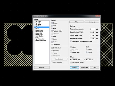
Configuring Gerber Export Settings
In the Gerber export settings window, you can customize various parameters to ensure your Gerber files are generated according to your requirements and the specifications provided by your PCB manufacturer. Here are some key settings to consider:
General Settings
- Format: Choose between “RS-274X” (extended Gerber) or “RS-274D” (standard Gerber). Most PCB manufacturers prefer the RS-274X format.
- Units: Select the appropriate unit system for your design, either “Inches” or “Millimeters.”
- Coordinate Format: Specify the coordinate format for the Gerber files. Common options include “2.3” (two integer digits and three decimal digits) and “2.4” (two integer digits and four decimal digits).
Apertures
- Aperture Table: Choose the aperture table format, such as “Embedded” (include aperture definitions in each Gerber file) or “Separate File” (generate a separate aperture file).
- Aperture Sizes: Review and modify the aperture sizes if necessary. Diptrace automatically assigns aperture sizes based on your design elements.
Output Files
In the “Output Files” section, you can select which layers to include in the Gerber export. Ensure that all the necessary layers are selected, such as:
- Top and bottom copper layers
- Solder mask layers
- Silkscreen layers
- Paste mask layers (if applicable)
- Board outline layer
- Drill files
Drill Settings
Configure the drill settings according to your requirements:
- Format: Choose between “Excellon” or “Gerber” drill file format. Excellon is the most common format.
- Units: Select the appropriate unit system for the drill files, either “Inches” or “Millimeters.”
- Zeros: Specify the leading and trailing zero suppression for the drill coordinates.
- Drill Holes: Ensure that all the necessary drill holes are included in the export.
Once you have reviewed and configured the Gerber export settings, click “Export” to generate the Gerber files.
Saving and Organizing Gerber Files
After exporting the Gerber files, it’s important to save and organize them properly. Create a dedicated folder for your Gerber files and ensure that all the generated files are stored together.
Diptrace will generate individual files for each layer and the drill data. The file names will typically include the layer name and the corresponding Gerber file extension. For example:
PCB_Name_TopCopper.gtlPCB_Name_BottomCopper.gblPCB_Name_TopSolderMask.gtsPCB_Name_BottomSolderMask.gbsPCB_Name_TopSilkscreen.gtoPCB_Name_BottomSilkscreen.gboPCB_Name_BoardOutline.gkoPCB_Name_Drills.txt(or.drlfor Excellon format)
Compress the Gerber files into a single ZIP archive before sending them to your PCB manufacturer. Most fabrication houses prefer to receive a single compressed file containing all the necessary Gerber files.

Verifying Gerber Files
Before submitting your Gerber files to the PCB manufacturer, it’s crucial to verify their integrity and ensure that they accurately represent your PCB design. There are several methods to verify your Gerber files:
Visual Inspection
Perform a visual inspection of your Gerber files using a Gerber viewer software. There are many free and commercial Gerber viewers available, such as:
- Gerbv (open-source, cross-platform)
- ViewMate (freeware, Windows)
- GC-Prevue (commercial, Windows)
Open each Gerber file in the viewer and carefully examine the layers, checking for any discrepancies or missing elements. Verify that the board outline, copper layers, solder mask, silkscreen, and drill holes are correctly represented.
Gerber File Analysis Tools
Use Gerber file analysis tools to check for common issues and potential manufacturing problems. These tools can help identify design rule violations, aperture mismatches, and other errors that may affect the manufacturability of your PCB.
Some popular Gerber file analysis tools include:
- DFM Now (free, online)
- PCBWay DFM Check (free, online)
- GerberCheck (commercial, Windows)
Upload your Gerber files to these tools and review the analysis reports. Address any flagged issues and regenerate the Gerber files if necessary.
Communication with PCB Manufacturer
Engage in open communication with your PCB manufacturer regarding their Gerber file requirements and design guidelines. Many fabrication houses provide online DFM (Design for Manufacturability) tools or offer free file checks before placing an order.
Take advantage of these services to ensure that your Gerber files meet the manufacturer’s specifications. Provide any additional information or clarifications requested by the manufacturer to avoid delays in the fabrication process.

Best Practices for Gerber File Export
To ensure a smooth and successful PCB manufacturing process, follow these best practices when exporting Gerber files from Diptrace:
-
Adhere to Manufacturer’s Guidelines: Familiarize yourself with the design guidelines and specifications provided by your chosen PCB manufacturer. Follow their recommendations for layer stackup, minimum feature sizes, clearances, and drill sizes.
-
Use Consistent Units: Maintain consistency in the units used throughout your PCB design and Gerber file export. Ensure that the units in Diptrace match the units specified in the Gerber export settings.
-
Include All Necessary Layers: Double-check that all the required layers are included in your Gerber file export. This typically includes the copper layers, solder mask, silkscreen, and drill files. Consult with your manufacturer if you are unsure about which layers to include.
-
Provide Descriptive File Names: Use descriptive and meaningful file names for your Gerber files. Include the PCB name, layer identifier, and Gerber file extension in the file name. This helps in organizing and identifying the files easily.
-
Compress Gerber Files: Always compress your Gerber files into a single ZIP archive before sending them to the manufacturer. This ensures that all the necessary files are bundled together and reduces the chances of missing or misplaced files.
-
Verify and Double-Check: Take the time to thoroughly verify your Gerber files before submitting them for manufacturing. Use Gerber viewers and analysis tools to catch any errors or discrepancies early in the process.
-
Communicate with Manufacturer: Maintain open communication with your PCB manufacturer. Provide them with any additional information, specifications, or special requirements for your PCB design. Be responsive to their queries and feedback to avoid delays and ensure a successful manufacturing outcome.
FAQ
1. What if I encounter issues while exporting Gerber files from Diptrace?
If you face any problems during the Gerber file export process in Diptrace, first ensure that your PCB design is complete and error-free. Double-check the Gerber export settings and verify that all the necessary layers are selected. If the issue persists, consult the Diptrace documentation or seek support from the Diptrace community forums.
2. Can I use other file formats instead of Gerber for PCB manufacturing?
While Gerber files are the most widely accepted format for PCB manufacturing, some manufacturers may support alternative file formats such as ODB++ or IPC-2581. However, Gerber remains the industry standard, and it is recommended to use Gerber files unless specifically requested otherwise by your manufacturer.
3. How do I know if my Gerber files meet the manufacturer’s requirements?
Most PCB manufacturers provide design guidelines and specifications on their website. Review these guidelines carefully and ensure that your PCB design and Gerber files adhere to their requirements. Many manufacturers also offer free DFM checks or online tools to validate your Gerber files before placing an order.
4. What should I do if my PCB manufacturer reports issues with my Gerber files?
If your PCB manufacturer identifies issues with your Gerber files, communicate with them to understand the specific problems. Request detailed feedback and suggestions for resolving the issues. Make the necessary corrections in your PCB design software and regenerate the Gerber files. Verify the updated files before resubmitting them to the manufacturer.
5. Can I include additional information or instructions with my Gerber files?
Yes, you can include additional information or special instructions for your PCB manufacturer. Create a separate text file or readme document outlining any specific requirements, such as material preferences, surface finishes, or testing procedures. Include this file along with your Gerber files when sending them to the manufacturer.
Conclusion
Exporting your Diptrace PCB design to Gerber files is a critical step in the PCB manufacturing process. By following the steps and best practices outlined in this guide, you can ensure that your Gerber files are accurate, complete, and ready for fabrication.
Remember to thoroughly verify your Gerber files, communicate with your PCB manufacturer, and adhere to their design guidelines to minimize issues and delays. With properly exported Gerber files, you can confidently send your PCB design for manufacturing and bring your electronic projects to life.
Leave a Reply