Introduction to QFN Packages and Soldering Challenges
Quad Flat No-lead (QFN) packages have become increasingly popular for integrated circuits due to their small size, good thermal and electrical performance, and low cost. However, the small lead pitch and hidden leads under the package make QFN soldering more challenging compared to other SMT packages.
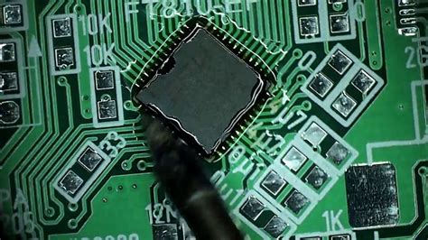
QFN packages have no visible leads and very small spacing between pads, typically 0.5mm or less. The leads are located under the body of the component. During reflow soldering, the solder joint is formed under the package, making it difficult to visually inspect. Voids in the solder joints under the thermal pad are another common issue that can affect reliability.
To achieve reliable QFN soldering, careful PCB layout is essential. This article discusses key considerations and recommendations for QFN footprint and board design to minimize common defects and improve manufacturability.
QFN Footprint Design Guidelines
Pad Size and Spacing
Proper sizing and spacing of the QFN land pattern is critical for robust solder joints. The PCB pads should be slightly larger than the component pads to allow for registration tolerances.
A typical recommendation is to make the PCB pads 0.05mm longer on each side compared to the QFN pads. This provides sufficient area for a good solder fillet to form. The width of the PCB pads can be the same as the component lead width.
The space between QFN pads is very small, often 0.5mm pitch or less. It’s important to maintain adequate spacing between adjacent pads to avoid solder bridging. A good rule of thumb is to keep at least 0.2mm between pads for 0.5mm pitch QFNs.
Here is an example of recommended pad sizing for a 0.5mm pitch QFN:
| QFN Lead Pitch | QFN Pad Length | PCB Pad Length | PCB Pad Width | Space Between Pads |
|---|---|---|---|---|
| 0.50mm | 0.35mm | 0.40mm | 0.25mm | 0.20mm |
Thermal Pad
Most QFN packages have an exposed thermal pad underneath for heat dissipation. This thermal pad is typically soldered directly to a copper plane on the PCB. Proper design of the thermal pad is important to minimize voiding.
The PCB thermal pad should match the size of the QFN thermal pad or be slightly (0.2-0.5mm) smaller on each side. Avoid making the PCB pad too large, as this can increase the risk of voiding.
For reliable soldering, the PCB thermal pad should include thermal vias to help conduct heat away from the package into internal copper layers. A typical via pattern is a grid of 0.3-0.5mm diameter vias evenly spaced at 1.2mm pitch across the thermal pad area.
Thermal vias help outgas flux vapors during reflow and minimize solder wicking down the holes. The vias should be filled or tented with solder mask to prevent solder loss.
Example of a QFN thermal pad with via pattern:
| QFN Thermal Pad Size | PCB Thermal Pad Size | Via Size | Via Pitch |
|---|---|---|---|
| 5.0mm x 5.0mm | 4.5mm x 4.5mm | 0.3mm | 1.2mm |
Solder Mask Clearance
Solder mask helps prevent solder bridging between pads and defines the solderable area. Clearance between the solder mask opening and copper pad is needed to account for registration tolerances.
For QFN designs, a solder mask opening that is 0.05-0.1mm larger than the copper pad on each side is typically recommended. This ensures the entire pad is solderable while minimizing solder spreading.
The solder mask opening for the thermal pad should match the size of the copper pad. The thermal vias should be tented or filled with solder mask to prevent solder wicking.

Stencil Design Considerations
Proper stencil design is critical for QFN soldering to ensure the right amount of solder paste is deposited on each pad. The small pad size and tight spacing of QFNs require a well-designed stencil.
Stencil Thickness
The stencil thickness determines the volume of solder paste deposited. For fine-pitch QFNs, a stencil thickness of 0.100-0.125mm (4-5 mils) is typically used. This provides enough solder volume for good joint formation without excessive solder.
Thinner stencils can be used but may result in insufficient solder volume. Thicker stencils deposit more solder but increase the risk of bridging.
Aperture Size and Shape
The stencil aperture should be slightly smaller than the pad size, typically by 0.05mm on each side. This reduces the risk of solder bridging while still providing enough solder volume.
For rectangular pads, the aperture shape should also be rectangular with rounded corners. The corners are typically rounded to 25-50% of the aperture width to facilitate solder paste release.
The thermal pad aperture requires special consideration. A large opening can cause solder beading and voiding. It’s common to divide the thermal pad aperture into a grid of smaller openings with 50-75% coverage. The individual openings are typically 0.75-2.0mm square with 0.5-1.0mm spacing between them.
Example of a QFN stencil design:
| Pad Size | Aperture Size | Aperture Shape | Thermal Pad Aperture |
|---|---|---|---|
| 0.4×0.25mm | 0.35×0.2mm | Rounded Rectangle | 4×4 grid of 1.0mm square openings with 0.75mm spacing |

Reflow Soldering Profile
The reflow soldering profile is another important factor in achieving reliable QFN solder joints. The small size and thermal mass of QFNs require precise control of peak temperature and time above liquidus (TAL).
Ramp Rate
A gradual ramp rate of 1-2°C/second is recommended for QFNs to allow the entire assembly to heat uniformly. This minimizes thermal stress and reduces the risk of tombstoning or component shifting.
Soak Zone
The soak zone is a temperature plateau between 150-180°C that activates the solder flux before melting occurs. A soak time of 60-90 seconds is typical for QFNs. The soak helps minimize voiding by allowing the flux to outgas before the solder melts.
Peak Temperature
The peak reflow temperature should be 20-40°C above the solder liquidus point to ensure complete melting. For common SAC305 solder, a peak of 245-260°C is recommended. Higher peak temperatures increase wetting and minimize voiding but also increase intermetallic growth. Lower peak temperatures reduce intermetallics but may not achieve complete solder melting.
The peak temperature should be tightly controlled to avoid damage to the QFN package or PCB. The QFN package datasheet will specify a maximum peak temperature that must not be exceeded.
Time Above Liquidus
The time above liquidus (TAL) is the duration that the solder is molten, and is critical for forming a good intermetallic bond. A TAL of 30-90 seconds is typically recommended for QFNs. Longer TAL improves wetting but increases the growth of brittle intermetallics. Shorter TAL may result in incomplete melting or poor wetting.
Example reflow profile for QFN with SAC305 solder:
| Zone | Target |
|---|---|
| Ramp | 1-2°C/sec |
| Soak | 150-180°C for 60-90sec |
| Peak | 245-260°C |
| Time Above 217°C | 30-90sec |

Inspection and Quality Control
Thorough inspection is important to verify QFN soldering quality and identify any defects or process issues. However, the hidden solder joints under the package make inspection challenging.
Visual Inspection
Visual inspection of QFN solder joints is limited to the side fillets. A well-formed fillet should be concave in shape and extend up the side of the package. Bulging fillets indicate excess solder while flat or concave fillets suggest insufficient solder volume.
Bridging between leads can also be detected visually. Solder should not extend beyond the edge of the pads.
Solder residue around the package may indicate incomplete flux activation or an unoptimized reflow profile.
X-Ray Inspection
X-ray inspection is the most effective method to verify hidden solder joints under the QFN package. 2D X-ray can detect gross voids, bridging, or missing solder but has limited resolution. 3D or CT X-ray provides greater insight into joint formation and void percentage.
Less than 25% voiding under the thermal pad is a common acceptability criterion. Voids should be dispersed rather than clustered in one area.
Head-in-pillow defects where the solder paste does not fully coalesce with the QFN lead are another defect detectable by X-ray. HIPs appear as a gray crescent at the edge of the lead.
Electrical Testing
Electrical tests like in-circuit test (ICT) or boundary scan can verify continuity and basic functionality of the soldered QFN. However, these tests may not detect defects like large thermal pad voids that could still impact long-term reliability.
Conclusion
QFNs are a popular package style but require careful PCB design and process control to achieve reliable solder joints. Key considerations include proper footprint design with sized pads and thermal vias, precision stencil printing with segmented thermal pad apertures, and a well-tuned reflow profile with adequate flux activation and controlled peak temperature.
Inspection methods like X-ray are essential to detect hidden solder defects under the package. By optimizing the board layout and assembly process for QFNs, high quality and reliability can be achieved in volume production.
Frequently Asked Questions
What are the most common QFN soldering defects?
Some of the most common QFN soldering defects include:
– Voiding under the thermal pad
– Bridging between leads
– Poor wetting or non-wetting of leads
– Head-in-pillow defects
– Tombstoning or component shifting
How much solder paste should be printed on QFN pads?
The volume of solder paste is determined by the stencil thickness and aperture size. A typical stencil thickness for QFNs is 0.1-0.125mm (4-5 mils). The aperture size is normally 0.05mm smaller than the pad size on each side to allow for registration tolerance while providing adequate solder volume.
What is the shelf life of solder paste?
Solder paste shelf life depends on the alloy composition and storage conditions but is typically 6-12 months when refrigerated. Solder paste should be allowed to warm to room temperature for several hours before use. Working life of solder paste after removal from the refrigerator is typically 1-2 months.
How do I select a reflow profile for my QFN board?
The reflow profile should be tailored to the thermal mass of the entire assembly, not just the QFN. A profile with a gradual ramp rate, soak zone to activate flux, peak temperature 20-40°C above solder liquidus, and TAL of 30-90sec is a good starting point. The exact profile should then be optimized based on inspection and quality data.
What is the maximum void percentage allowed for QFN solder joints?
Industry standards like IPC-610 allow up to 25% voiding under QFN thermal pads as long as the voids are dispersed. Some automotive or aerospace specifications are stricter and may require less than 15% voiding. The acceptability of voids depends on the specific application and reliability requirements.
Leave a Reply