Introduction to Flex-Rigid PCBs
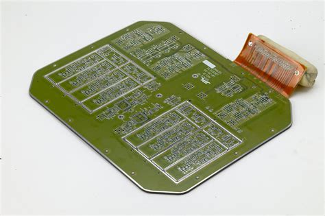
Flex-rigid PCBs are a unique type of printed circuit board that combines the best features of both flexible and rigid PCBs. These hybrid boards consist of multiple layers of flexible and rigid substrates that are laminated together into a single structure. This innovative technology offers numerous advantages over traditional PCBs, including improved reliability, reduced size and weight, and enhanced design flexibility.
What are Flex-Rigid PCBs?
A flex-rigid PCB is a printed circuit board that incorporates both flexible and rigid substrates. The flexible portions are typically made from polyimide or other thin, bendable materials, while the rigid sections are constructed from standard FR-4 or similar rigid substrates. The flexible and rigid layers are interconnected using plated through-holes (PTHs) and other methods to create a seamless, integrated circuit board.
Advantages of Flex-Rigid PCBs
Flex-rigid PCBs offer several key advantages over traditional rigid PCBs:
- Space savings: By combining flexible and rigid sections, flex-rigid PCBs can be folded, bent, or shaped to fit into tight spaces, reducing the overall size and weight of the device.
- Improved reliability: The flexible portions of the PCB can absorb stress and vibration, reducing the risk of damage to components and connections.
- Enhanced design flexibility: Flex-rigid PCBs allow for more creative and efficient layouts, as the flexible sections can be routed around obstacles or conform to unusual shapes.
- Reduced assembly time and cost: By integrating multiple circuits into a single board, flex-rigid PCBs can simplify assembly processes and reduce the number of connectors required, lowering overall manufacturing costs.
Flex-Rigid PCB Manufacturing Process
The manufacturing process for flex-rigid PCBs is more complex than that of standard rigid PCBs, as it involves the integration of flexible and rigid materials. The following steps outline the general process for creating a flex-rigid PCB:
Step 1: Design and Layout
The first step in manufacturing a flex-rigid PCB is to create the design and layout using specialized PCB design software. The design must take into account the specific requirements of the flexible and rigid sections, including bend radii, layer stackup, and material selection.
Step 2: Material Selection
Next, the appropriate materials for the flexible and rigid sections must be chosen. Common flexible substrates include polyimide, polyester, and PTFE, while rigid sections typically use FR-4, aluminum, or ceramic substrates. The choice of materials will depend on the specific application, environmental conditions, and performance requirements of the PCB.
Step 3: Substrate Preparation
Once the materials have been selected, the flexible and rigid substrates must be prepared for lamination. This may involve cleaning, roughening, or applying adhesive coatings to ensure proper bonding between the layers.
Step 4: Lamination
The prepared flexible and rigid substrates are then laminated together using heat and pressure. The exact lamination process will depend on the materials used and the desired properties of the final PCB. Careful control of temperature, pressure, and time is essential to ensure a strong, reliable bond between the layers.
Step 5: Drilling and Plating
After lamination, the PCB is drilled to create vias and other openings for components and connections. The drilled holes are then plated with copper to create electrical pathways between layers. Special care must be taken when drilling and plating flex-rigid PCBs to avoid damaging the flexible sections.
Step 6: Patterning and Etching
The copper layers of the PCB are then patterned and etched to create the desired circuit traces and pads. This process typically involves applying a photoresist coating, exposing the resist to UV light through a photomask, and then developing and etching away the unwanted copper.
Step 7: Solder Mask Application
A solder mask is applied to the PCB to protect the copper traces and prevent short circuits during soldering. The solder mask is usually applied using a screen printing or photoimaging process.
Step 8: Surface Finish
Finally, a surface finish is applied to the exposed copper areas of the PCB to improve solderability and protect against oxidation. Common surface finishes include HASL (hot air solder leveling), ENIG (electroless nickel immersion gold), and OSP (organic solderability preservative).

Flex-Rigid PCB Layer Stackup
The layer stackup of a flex-rigid PCB is a critical aspect of the design process, as it determines the electrical, mechanical, and thermal properties of the board. A typical flex-rigid PCB Stackup consists of alternating layers of flexible and rigid substrates, with copper foil laminated to one or both sides of each layer.
| Layer | Material | Thickness (mm) | Description |
|---|---|---|---|
| 1 | Polyimide | 0.025 | Flexible substrate |
| 2 | Copper | 0.018 | Copper foil (one side) |
| 3 | FR-4 | 0.2 | Rigid substrate |
| 4 | Copper | 0.035 | Copper foil (both sides) |
| 5 | Polyimide | 0.025 | Flexible substrate |
| 6 | Copper | 0.018 | Copper foil (one side) |
The number and arrangement of layers can vary depending on the specific requirements of the application. Some common flex-rigid PCB stackups include:
- Rigid-Flex-Rigid: A flexible layer sandwiched between two rigid layers
- Flex-Rigid-Flex: A rigid layer sandwiched between two flexible layers
- Multi-layer Flex-Rigid: Multiple alternating layers of flexible and rigid substrates

Designing for Flex-Rigid PCBs
Designing a flex-rigid PCB requires careful consideration of several factors to ensure optimal performance and reliability. Some key design guidelines include:
Bend Radius
The bend radius is the minimum radius that the flexible portion of the PCB can be bent without causing damage. The bend radius is determined by the thickness and material properties of the flexible substrate, as well as the location and orientation of copper traces and components. It is important to design the PCB layout to accommodate the required bend radius and to avoid placing components or traces too close to the bend area.
Flexible-to-Rigid Transition
The transition between the flexible and rigid sections of the PCB is a critical area that requires special attention. Proper design of the transition area can help to minimize stress and prevent delamination or cracking of the PCB. Some common techniques for improving the transition include:
- Using a gradual taper or chamfer to reduce stress concentrations
- Adding strain relief features such as slots or cutouts
- Using a staggered or stepped transition to distribute stress more evenly
Component Placement
When placing components on a flex-rigid PCB, it is important to consider the location and orientation of the components relative to the flexible and rigid sections. Components should be placed in the rigid sections whenever possible to minimize stress on the solder joints. If components must be placed in the flexible sections, they should be oriented such that the solder joints are perpendicular to the direction of flexing to minimize stress.
Trace Routing
Trace routing on a flex-rigid PCB requires careful consideration of the mechanical stresses that the traces will be subjected to. Traces should be routed to minimize the number of bends and to avoid sharp corners or tight radii. In the flexible sections, traces should be routed perpendicular to the direction of flexing to minimize stress. It may also be necessary to use thicker or wider traces in the flexible sections to improve mechanical strength.

Applications of Flex-Rigid PCBs
Flex-rigid PCBs are used in a wide range of applications where space is limited, and reliability is critical. Some common applications include:
Aerospace and Defense
Flex-rigid PCBs are widely used in aerospace and defense applications, where they offer several key advantages. The ability to fold and bend the PCB allows for more efficient use of space in tight confines, such as aircraft cockpits or satellite payloads. The improved reliability and resistance to vibration and shock also make flex-rigid PCBs well-suited for use in harsh environments.
Medical Devices
Medical devices such as wearable monitors, implantable sensors, and surgical instruments often require compact, lightweight, and reliable electronics. Flex-rigid PCBs can be designed to conform to the shape of the device, allowing for more ergonomic and comfortable designs. The improved reliability and resistance to flexing and bending also make flex-rigid PCBs ideal for use in devices that may be subjected to frequent movement or stress.
Consumer Electronics
Flex-rigid PCBs are increasingly being used in consumer electronics, such as smartphones, tablets, and wearable devices. The ability to fold and bend the PCB allows for more creative and space-efficient designs, while the improved reliability and durability help to extend the lifespan of the device.
Automotive Electronics
Flex-rigid PCBs are also finding use in automotive electronics, particularly in applications such as instrument clusters, infotainment systems, and sensors. The ability to conform to irregular shapes and the improved resistance to vibration and temperature extremes make flex-rigid PCBs well-suited for use in the harsh environment of a vehicle.
Frequently Asked Questions (FAQ)
Q1: What is the difference between a flex PCB and a flex-rigid PCB?
A: A flex PCB is a printed circuit board made entirely from flexible materials, while a flex-rigid PCB combines both flexible and rigid materials into a single board. Flex-rigid PCBs offer the advantages of both types of PCBs, including improved reliability, reduced size and weight, and enhanced design flexibility.
Q2: Can flex-rigid PCBs be repaired?
A: Repairing a flex-rigid PCB can be challenging due to the complex nature of the board and the presence of both flexible and rigid sections. In many cases, it may be more cost-effective to replace the entire board rather than attempting a repair. However, if a repair is necessary, it should be performed by a skilled technician using specialized tools and techniques to avoid damaging the board.
Q3: What is the maximum number of layers in a flex-rigid PCB?
A: The maximum number of layers in a flex-rigid PCB depends on the specific design and manufacturing capabilities of the PCB fabricator. Some manufacturers can produce flex-rigid PCBs with up to 30 layers or more, while others may be limited to fewer layers. The number of layers also affects the overall thickness and flexibility of the board.
Q4: How do you specify the bend radius for a flex-rigid PCB?
A: The bend radius for a flex-rigid PCB is typically specified as a multiple of the thickness of the flexible substrate. For example, a bend radius of 10T means that the minimum bend radius is 10 times the thickness of the flexible layer. The exact bend radius will depend on the specific materials and design of the PCB, and should be determined in consultation with the PCB manufacturer.
Q5: What are the typical lead times for flex-rigid PCBs?
A: Lead times for flex-rigid PCBs can vary depending on the complexity of the design, the materials used, and the volume of the order. In general, lead times for flex-rigid PCBs are longer than for standard rigid PCBs due to the additional processing steps and specialized equipment required. Typical lead times can range from 3-4 weeks for simple designs to 8-10 weeks or more for complex, high-volume orders. It is important to work closely with the PCB manufacturer to determine realistic lead times and to plan accordingly.
Conclusion
Flex-rigid PCBs are a powerful technology that offers numerous advantages over traditional rigid PCBs. By combining the benefits of both flexible and rigid substrates, flex-rigid PCBs enable more compact, lightweight, and reliable designs that can withstand the rigors of harsh environments and frequent flexing.
However, designing and manufacturing flex-rigid PCBs requires specialized knowledge and expertise. Careful consideration must be given to factors such as bend radius, layer stackup, component placement, and trace routing to ensure optimal performance and reliability.
As the demand for smaller, more complex, and more reliable electronic devices continues to grow, flex-rigid PCBs will play an increasingly important role in a wide range of applications, from aerospace and defense to medical devices and consumer electronics. By staying up-to-date with the latest advancements in flex-rigid PCB technology and working closely with experienced PCB manufacturers like RAYPCB, designers and engineers can unlock new possibilities and push the boundaries of what is possible in electronic packaging and interconnect.
Leave a Reply