Understand the Importance of PCB Design Guidelines
PCB design guidelines are a set of rules and best practices that help designers create printed circuit boards that meet the required specifications and perform optimally. These guidelines cover various aspects of PCB design, including component placement, routing, signal integrity, power distribution, and manufacturability.
Following PCB design guidelines is essential because it helps to:
- Ensure the reliability and functionality of the PCB
- Minimize the risk of design errors and manufacturing issues
- Reduce the overall cost of production
- Improve the efficiency and performance of the PCB
- Facilitate easier debugging and maintenance
Consider the PCB’s Purpose and Environment
Before starting the PCB design process, it is crucial to understand the purpose and environment in which the PCB will operate. This information will help you make informed decisions about the PCB’s layout, component selection, and manufacturing requirements.
Consider the following factors:
- The intended application of the PCB (e.g., consumer electronics, automotive, medical, etc.)
- The expected operating conditions (e.g., temperature, humidity, vibration, etc.)
- The power requirements and voltage levels
- The required level of reliability and durability
- Any specific industry standards or regulations that need to be met

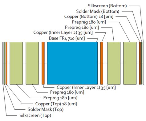
Choose the Right PCB Material and Thickness
The choice of PCB material and thickness is critical for ensuring the PCB’s performance and reliability. The most common PCB materials are FR-4, Rogers, and Polyimide, each with its own unique properties and advantages.
| Material | Properties | Applications |
|---|---|---|
| FR-4 | – Low cost – Good mechanical strength – Suitable for most applications |
– Consumer electronics – Industrial control systems |
| Rogers | – Low dielectric loss – Stable at high frequencies – Excellent thermal conductivity |
– High-frequency applications – RF and microwave circuits |
| Polyimide | – High heat resistance – Flexible and lightweight – Good chemical resistance |
– Aerospace and military applications – Flexible electronics |
The thickness of the PCB is also important, as it affects the board’s mechanical strength, thermal dissipation, and impedance control. Common PCB thicknesses range from 0.4mm to 3.2mm, with 1.6mm being the most widely used.

Follow Proper Component Placement and Orientation
Proper component placement and orientation are essential for ensuring the PCB’s functionality, manufacturability, and reliability. Here are some guidelines to follow:
- Place components in a logical and organized manner, grouping related components together
- Minimize the distance between connected components to reduce signal loss and interference
- Orient components in the same direction whenever possible to facilitate automated assembly
- Ensure adequate spacing between components for proper soldering and heat dissipation
- Consider the component’s height and placement on both sides of the board to avoid mechanical interference

Implement Effective Power Distribution and Grounding
Power distribution and grounding are critical aspects of PCB design that directly impact the board’s performance and signal integrity. Here are some guidelines to follow:
- Use appropriate trace widths for power and ground connections based on the expected current flow
- Implement a solid ground plane to provide a low-impedance return path for signals
- Decouple power supplies using appropriate capacitors to minimize noise and ensure stable power delivery
- Use separate power and ground planes for analog and digital circuits to avoid crosstalk and interference
- Implement proper power sequencing to prevent damage to components during power-up and power-down
Optimize Signal Routing and Integrity
Signal routing and integrity are crucial for ensuring the PCB’s functionality and reliability. Here are some guidelines to follow:
- Keep signal traces as short and direct as possible to minimize signal loss and distortion
- Maintain consistent trace widths and spacings to ensure controlled impedance and minimize signal reflections
- Avoid sharp corners and use 45-degree angles or curved traces to reduce signal reflections
- Implement proper termination techniques, such as series and parallel termination, to maintain signal integrity
- Use appropriate shielding and grounding techniques to minimize crosstalk and electromagnetic interference (EMI)
Consider Manufacturability and Assembly
Designing a PCB with manufacturability and assembly in mind can help reduce production costs and improve the overall quality of the finished product. Here are some guidelines to follow:
- Adhere to the manufacturer’s design rules and guidelines for minimum trace widths, spacings, and hole sizes
- Provide adequate clearances around components and connectors for automated assembly equipment
- Use standard component sizes and packages whenever possible to minimize custom parts and reduce costs
- Include fiducial markers and alignment holes to facilitate accurate component placement during assembly
- Provide clear and concise assembly instructions, including component orientations and special handling requirements
Conduct Thorough Design Reviews and Testing
Conducting thorough design reviews and testing is essential for catching and correcting any design errors or issues before the PCB goes into production. Here are some guidelines to follow:
- Perform a design rule check (DRC) to ensure the PCB layout adheres to the manufacturer’s design rules and guidelines
- Conduct a schematic review to verify the accuracy of the circuit design and component connections
- Perform a 3D mechanical check to ensure proper component clearances and avoid any mechanical interferences
- Conduct signal integrity simulations to verify the performance of critical signals and identify any potential issues
- Perform functional testing on prototype boards to validate the PCB’s functionality and performance
Stay Updated with Industry Standards and Best Practices
PCB design is an ever-evolving field, with new technologies, materials, and techniques constantly emerging. To stay competitive and ensure the highest quality PCB designs, it is essential to stay updated with industry standards and best practices.
Some ways to stay informed include:
- Attending PCB design conferences and workshops
- Participating in online forums and communities dedicated to PCB design
- Reading industry publications and blogs
- Staying current with the latest design software and tools
- Collaborating with experienced PCB designers and engineers
Frequently Asked Questions (FAQ)
-
What is the importance of following PCB design guidelines?
Following PCB design guidelines ensures the reliability, functionality, and cost-effectiveness of the printed circuit board. It helps minimize design errors, manufacturing issues, and improves the overall performance of the PCB. -
How do I choose the right PCB material for my application?
The choice of PCB material depends on the specific requirements of your application, such as the operating environment, frequency range, and required level of reliability. Common PCB materials include FR-4, Rogers, and Polyimide, each with its own unique properties and advantages. -
What are some key considerations for component placement and orientation?
When placing components on a PCB, it is important to group related components together, minimize the distance between connected components, orient components in the same direction whenever possible, ensure adequate spacing for soldering and heat dissipation, and consider the component’s height and placement on both sides of the board. -
How can I optimize power distribution and grounding in my PCB design?
To optimize power distribution and grounding, use appropriate trace widths for power and ground connections, implement a solid ground plane, decouple power supplies using appropriate capacitors, use separate power and ground planes for analog and digital circuits, and implement proper power sequencing. -
What are some best practices for ensuring manufacturability and assembly?
To ensure manufacturability and assembly, adhere to the manufacturer’s design rules and guidelines, provide adequate clearances around components and connectors, use standard component sizes and packages whenever possible, include fiducial markers and alignment holes, and provide clear and concise assembly instructions.
By following these PCB design guidelines and staying informed about industry best practices, you can create high-quality, reliable, and cost-effective printed circuit boards that meet the specific requirements of your application. Remember, investing time and effort into proper PCB design can save you significant time and money in the long run by minimizing design errors, manufacturing issues, and improving the overall performance of your product.
Leave a Reply