What are Gerber Files and Why Do You Need Them?
Gerber files are the standard file format used in the printed circuit board (PCB) industry for manufacturing. They contain all the necessary information for fabricating a PCB, including the copper layers, solder mask, silkscreen, and drill data. When you design a PCB using KiCad, you need to generate Gerber files to send to a PCB manufacturer for production.
Gerber File Types
There are several types of Gerber files, each representing a different layer or aspect of the PCB:
| File Extension | Description |
|---|---|
| .GTL | Top copper layer |
| .GBL | Bottom copper layer |
| .GTS | Top solder mask |
| .GBS | Bottom solder mask |
| .GTO | Top silkscreen |
| .GBO | Bottom silkscreen |
| .TXT | Drill data |
| .GKO | Board outline |
Step-by-Step Guide to Exporting Gerber Files in KiCad
Follow these steps to generate Gerber files from your KiCad PCB design:
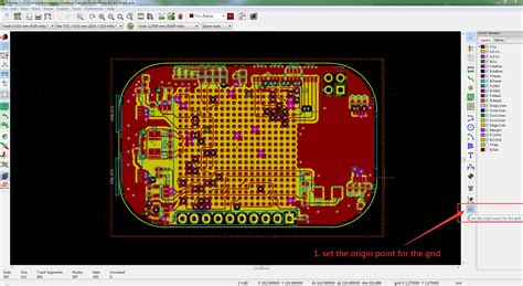
Step 1: Open the PCB Layout Editor
- Open your KiCad project and navigate to the PCB layout editor by double-clicking on the .kicad_pcb file in the project tree.
Step 2: Run DRC (Design Rule Check)
- Before generating Gerber files, it’s essential to run a Design Rule Check (DRC) to ensure your PCB design adheres to the manufacturer’s specifications and design rules.
- In the PCB layout editor, click on the “Run DRC” button in the top toolbar or go to “Tools” > “DRC…”.
- Configure the DRC settings according to your manufacturer’s requirements and click “Run DRC”.
- If any errors or warnings are found, address them before proceeding.
Step 3: Open the Plot Dialog
- In the PCB layout editor, click on “File” > “Plot…” to open the plot dialog.
Step 4: Configure the Plot Settings
- In the plot dialog, set the “Output directory” to a location where you want to save the Gerber files.
- Under “Plot format”, select “Gerber”.
- In the “General Options” tab, ensure that “Plot border and title block” is unchecked and “Exclude PCB Edge layer from other layers” is checked.
- In the “Layers” tab, select the layers you want to include in the Gerber files. Typically, you’ll need to include the following layers:
- F.Cu (Top copper)
- B.Cu (Bottom copper)
- F.SilkS (Top silkscreen)
- B.SilkS (Bottom silkscreen)
- F.Mask (Top solder mask)
- B.Mask (Bottom solder mask)
- Edge.Cuts (Board outline)
- Click on “Plot” to generate the Gerber files.
Step 5: Generate Drill Files
- In the plot dialog, click on the “Generate Drill Files…” button.
- In the drill file dialog, set the “Output directory” to the same location where you saved the Gerber files.
- Under “Drill Units”, select “Inches” or “Millimeters” according to your manufacturer’s requirements.
- Click on “Generate Drill File” to create the drill files.
Step 6: Review and Verify the Gerber Files
- After generating the Gerber and drill files, it’s crucial to review and verify them before sending them to the manufacturer.
- Open the Gerber files using a Gerber viewer, such as gerbv or the online viewer provided by your PCB manufacturer.
- Check each layer for any errors, missing features, or incorrect dimensions.
- Ensure that the drill files align properly with the copper layers.

Tips for Successful Gerber File Generation
- Always run a DRC before generating Gerber files to catch any design issues early.
- Double-check your manufacturer’s requirements for Gerber file format, units, and layer specifications.
- Use a consistent naming convention for your Gerber files to avoid confusion.
- Verify your Gerber files using a reliable Gerber viewer before submitting them for production.
- Include a README file with your Gerber files, providing any additional information or special instructions for the manufacturer.

Frequently Asked Questions (FAQ)
-
Q: What if I encounter errors while running DRC in KiCad?
A: If you encounter DRC errors, it means there are design issues that need to be resolved before generating Gerber files. Review the error messages, locate the problematic areas in your PCB layout, and make the necessary corrections. Common issues include incorrect clearances, overlapping traces, or missing connections. -
Q: Can I include custom layers in my Gerber files?
A: Yes, KiCad allows you to include custom layers in your Gerber files. In the plot dialog, you can select any additional layers you’ve created in your PCB design. However, make sure to communicate with your manufacturer about any custom layers to ensure they can accommodate them in their fabrication process. -
Q: What should I do if my manufacturer requires specific Gerber file settings?
A: If your PCB manufacturer has specific requirements for Gerber file settings, such as file format, units, or layer specifications, make sure to follow their guidelines closely. Consult their documentation or reach out to their support team for clarification if needed. Adhering to their requirements will help ensure a smooth and accurate manufacturing process. -
Q: How can I check if my Gerber files are correctly generated?
A: To verify the correctness of your Gerber files, you can use a Gerber viewer tool. There are several free and commercial Gerber viewers available, such as gerbv, GerberLogix, or the online viewers provided by PCB manufacturers. These tools allow you to visualize each layer of your PCB and check for any discrepancies or errors. -
Q: What should I include in the README file with my Gerber files?
A: When submitting Gerber files to a PCB manufacturer, it’s helpful to include a README file that provides additional information and instructions. In the README file, you can specify: - The PCB dimensions and thickness
- The desired solder mask and silkscreen colors
- Any special requirements or notes for the manufacturer
- Your contact information in case they need to reach out for clarification
Including a README file helps ensure clear communication with the manufacturer and reduces the chances of misunderstandings or delays in the production process.

Conclusion
Exporting Gerber files from your KiCad PCB design is a crucial step in the PCB fabrication process. By following the step-by-step guide provided in this article, you can generate accurate and complete Gerber files that meet your manufacturer’s requirements. Remember to run a DRC before generating the files, select the appropriate layers, and verify the files using a Gerber viewer. Additionally, consider the tips and frequently asked questions discussed to ensure a smooth and successful PCB manufacturing experience. With properly generated Gerber files, you can confidently send your PCB design to the manufacturer and bring your electronic projects to life.
Leave a Reply