Introduction to PCB Samples
When it comes to designing and manufacturing printed circuit boards (PCBs), having access to high-quality PCB samples is crucial. PCB samples allow designers, engineers, and manufacturers to test and evaluate the performance, reliability, and functionality of their designs before mass production. In this article, we will explore the importance of PCB samples, the different types of samples available, and how to effectively utilize them in the PCB design and manufacturing process.
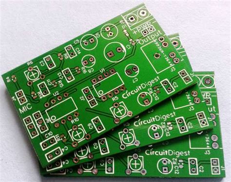
What are PCB Samples?
PCB samples are small-scale, functional representations of a complete PCB design. They are created to test and validate various aspects of the PCB, such as:
- Material selection
- Component placement
- Signal integrity
- Thermal management
- Manufacturing processes
By using PCB samples, designers and manufacturers can identify and address potential issues early in the development cycle, saving time and resources in the long run.
Types of PCB Samples
There are several types of PCB samples, each serving a specific purpose in the design and manufacturing process. Some common types include:
Prototype PCBs
Prototype PCBs are fully functional, small-batch PCBs that closely resemble the final product. They are used to test and validate the complete design, including component placement, routing, and functionality. Prototype PCBs are often used for:
- Proof-of-concept demonstrations
- Functional testing
- Firmware development
- Compliance testing
Bare Board PCBs
Bare board PCBs are PCBs without any components attached. They are used to test and evaluate the quality of the PCB fabrication process, including:
- Copper thickness
- Hole size and placement
- Solder mask application
- Silk screen printing
Bare board PCBs help ensure that the foundation of the PCB is sound before moving on to component assembly.
Assembly PCBs
Assembly PCBs are bare board PCBs with components attached. They are used to test and validate the component placement, soldering quality, and overall assembly process. Assembly PCBs help identify potential issues related to:
- Component compatibility
- Soldering defects
- Mechanical stress
- Thermal management
By using assembly PCBs, manufacturers can optimize their assembly processes and ensure the reliability of the final product.
The Importance of PCB Samples in the Design Process
PCB samples play a crucial role in the design process, allowing designers to test and refine their designs before committing to mass production. Some key benefits of using PCB samples in the design process include:
Design Validation
PCB samples allow designers to validate their designs in a real-world context. By testing the functionality, signal integrity, and thermal performance of the PCB, designers can identify and address potential issues early in the development cycle. This helps to reduce the risk of costly redesigns and production delays.
Component Selection
PCB samples can also be used to evaluate and select components for the final design. By testing different components on the sample PCB, designers can assess their performance, compatibility, and reliability. This helps to ensure that the final product meets the required specifications and performance criteria.
Manufacturing Process Optimization
PCB samples can be used to optimize the manufacturing process, including PCB fabrication and component assembly. By testing different manufacturing techniques and parameters on the sample PCBs, manufacturers can identify the most efficient and reliable processes for mass production. This helps to reduce manufacturing costs, improve yield rates, and ensure consistent product quality.

Effective Utilization of PCB Samples
To effectively utilize PCB samples in the design and manufacturing process, consider the following best practices:
Define Clear Objectives
Before creating PCB samples, clearly define the objectives and scope of the testing process. Identify the specific aspects of the design and manufacturing process that need to be evaluated, and prioritize them based on their impact on the final product.
Create Detailed Test Plans
Develop detailed test plans that outline the specific tests to be performed on the PCB samples, including the test conditions, equipment, and acceptance criteria. This helps to ensure that the testing process is comprehensive, repeatable, and aligned with the project objectives.
Document and Analyze Results
Carefully document and analyze the results of the PCB sample testing process. Identify any issues or areas for improvement and use this information to refine the design and manufacturing process. Maintain a record of the testing results for future reference and continuous improvement.
Collaborate with Stakeholders
Collaborate closely with all stakeholders involved in the PCB design and manufacturing process, including designers, engineers, manufacturers, and suppliers. Share the PCB sample testing results and gather feedback to ensure that everyone is aligned and working towards the same goals.

PCB Sample Case Studies
To illustrate the importance and effectiveness of PCB samples, let’s explore two real-world case studies.
Case Study 1: Automotive Infotainment System
An automotive electronics manufacturer was developing a new infotainment system for a luxury vehicle. The system required a high-density, multi-layer PCB with strict requirements for signal integrity and EMI/EMC performance.
The manufacturer created a series of PCB samples to test and validate the design, including:
- Bare board samples to evaluate the PCB fabrication quality
- Assembly samples to test the component placement and soldering process
- Functional prototypes to validate the system performance and compatibility
Through the PCB sample testing process, the manufacturer identified several issues, including signal integrity problems caused by improper routing and component placement. By addressing these issues early in the development cycle, the manufacturer was able to optimize the design and manufacturing process, resulting in a high-quality, reliable infotainment system that met all the required specifications.
Case Study 2: Medical Device PCB
A medical device company was developing a new PCB for a portable glucose monitoring system. The PCB needed to be compact, low-power, and highly reliable to ensure accurate glucose measurements and patient safety.
The company created a series of PCB samples to test and validate the design, including:
- Prototype samples to evaluate the PCB functionality and performance
- Assembly samples to test the component placement and soldering quality
- Compliance samples to ensure that the PCB met all relevant medical device regulations and standards
Through the PCB sample testing process, the company identified several areas for improvement, including the need for better thermal management to ensure stable performance in different environmental conditions. By incorporating these improvements into the final design, the company was able to create a highly accurate and reliable glucose monitoring system that met all the necessary regulatory requirements.

FAQ
- What are the benefits of using PCB samples in the design process?
-
PCB samples allow designers to validate their designs, test component selection, and optimize the manufacturing process early in the development cycle, reducing the risk of costly redesigns and production delays.
-
What are the different types of PCB samples?
-
Common types of PCB samples include prototype PCBs, bare board PCBs, and assembly PCBs, each serving a specific purpose in the design and manufacturing process.
-
How can PCB samples help optimize the manufacturing process?
-
PCB samples can be used to test different manufacturing techniques and parameters, helping manufacturers identify the most efficient and reliable processes for mass production, reducing costs, and improving yield rates.
-
What should be included in a PCB sample test plan?
-
A PCB sample test plan should outline the specific tests to be performed, including the test conditions, equipment, and acceptance criteria, ensuring that the testing process is comprehensive, repeatable, and aligned with project objectives.
-
How can collaboration improve the PCB sample testing process?
- Collaborating closely with all stakeholders involved in the PCB design and manufacturing process, sharing testing results, and gathering feedback helps ensure that everyone is aligned and working towards the same goals, leading to better outcomes and continuous improvement.
Conclusion
PCB samples are an essential tool in the design and manufacturing of high-quality, reliable printed circuit boards. By providing a means to test and validate designs, select components, and optimize manufacturing processes, PCB samples help to reduce development costs, improve product quality, and accelerate time-to-market.
To effectively utilize PCB samples, it is important to define clear objectives, create detailed test plans, document and analyze results, and collaborate closely with all stakeholders involved in the PCB design and manufacturing process. By following these best practices and leveraging the insights gained from PCB sample testing, designers and manufacturers can create innovative, high-performance PCBs that meet the demands of today’s complex electronic systems.
Leave a Reply