Introduction to PCB Panelization
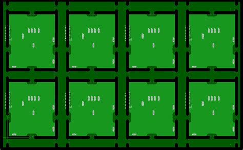
PCB panelization is the process of combining multiple printed circuit board designs onto a single panel for manufacturing. This technique is widely used in the electronics industry to reduce production costs, improve efficiency, and streamline the assembly process. By panelizing PCBs, manufacturers can produce a larger number of boards in a single run, minimizing material waste and setup time.
Computer-Aided Manufacturing (CAM) software plays a crucial role in the panelization process. CAM tools allow designers and engineers to create optimized panel layouts, define tooling and routing paths, and generate the necessary files for manufacturing. In this article, we will explore the various aspects of panelizing PCBs using CAM software and provide a comprehensive guide to help you achieve the best results.
Key Benefits of PCB Panelization
Panelizing PCBs offers several advantages to both manufacturers and customers. Some of the key benefits include:
-
Cost Reduction: By producing multiple PCBs on a single panel, manufacturers can minimize material waste, reduce setup time, and optimize machine utilization. This leads to lower production costs, which can be passed on to customers.
-
Increased Efficiency: Panelization streamlines the manufacturing process by allowing for the production of a larger number of boards in a single run. This reduces the need for frequent tooling changes and minimizes downtime, resulting in improved overall efficiency.
-
Consistent Quality: When PCBs are panelized, they undergo the same manufacturing processes simultaneously. This ensures consistent quality across all the boards on the panel, reducing the likelihood of variations or defects.
-
Simplified Assembly: Panelized PCBs are designed with assembly in mind. They often include features such as tooling holes, fiducial marks, and breakaway tabs, which facilitate automated assembly processes and reduce the risk of errors.

Factors to Consider When Panelizing PCBs
Before diving into the panelization process, it’s essential to consider several factors that can impact the success of your project. These factors include:
PCB Design
The individual PCB designs that will be panelized should be optimized for the panelization process. This involves ensuring that the boards have adequate spacing between them, proper placement of components, and the inclusion of necessary features such as tooling holes and fiducial marks.
Panel Size and Material
The size and material of the panel should be carefully selected based on the specific requirements of your project. Common panel sizes include 18″ x 24″ (457mm x 610mm) and 21″ x 24″ (533mm x 610mm), but custom sizes can also be accommodated. The choice of material, such as FR-4, Rogers, or aluminum, depends on the intended application and performance requirements of the PCBs.
Tooling and Routing Considerations
When panelizing PCBs, it’s crucial to consider the tooling and routing requirements. This includes the placement of tooling holes, which are used for alignment and registration during the manufacturing process. Additionally, the routing paths for separating the individual boards from the panel should be carefully planned to ensure clean and accurate breakouts.
Manufacturing Capabilities
The panelization process should take into account the capabilities of the manufacturing facility. This includes the available equipment, such as CNC routers, laser cutters, and pick-and-place machines, as well as the expertise of the personnel. It’s essential to collaborate closely with the manufacturing team to ensure that the panelized design can be efficiently produced.

Steps in the PCB Panelization Process
The PCB panelization process typically involves the following steps:
-
Design Preparation: The individual PCB designs are reviewed and optimized for panelization. This includes ensuring proper spacing, component placement, and the inclusion of necessary features.
-
Panel Layout Creation: Using CAM software, the individual PCB designs are arranged on a single panel. The layout takes into account factors such as board orientation, spacing, and tooling requirements.
-
Tooling and Routing Definition: The locations of tooling holes and the routing paths for separating the individual boards are defined in the CAM software. This step ensures accurate registration and clean breakouts during the manufacturing process.
-
Gerber File Generation: Once the panel layout is finalized, the CAM software generates the necessary Gerber files for manufacturing. These files include the copper layers, solder mask, silkscreen, and drilling information.
-
Manufacturing: The generated Gerber files are sent to the manufacturing facility, where the panels are fabricated using the specified materials and processes. The individual PCBs are then separated from the panel using the defined routing paths.
-
Quality Control: After manufacturing, the panelized PCBs undergo a thorough quality control process to ensure that they meet the required specifications and are free from defects.

Best Practices for PCB Panelization
To ensure successful PCB panelization, consider the following best practices:
-
Maintain Adequate Spacing: Provide sufficient spacing between the individual PCBs on the panel to allow for clean breakouts and to minimize the risk of damage during the depaneling process.
-
Use Standardized Panel Sizes: Whenever possible, use standardized panel sizes to optimize material usage and reduce costs. Common panel sizes are readily available from most manufacturers.
-
Include Fiducial Marks: Incorporate fiducial marks on the panel to facilitate accurate alignment and registration during the assembly process. These marks serve as reference points for automated pick-and-place machines.
-
Plan for Tooling Holes: Include tooling holes in the panel design to aid in alignment and registration during the manufacturing process. The size and placement of these holes should be based on the specific requirements of the manufacturing equipment.
-
Consider Depaneling Methods: Select an appropriate depaneling method based on the design and material of the PCBs. Common methods include V-scoring, tab routing, and pizza-cutting. Each method has its advantages and limitations, so choose the one that best suits your project.
-
Collaborate with the Manufacturing Team: Work closely with the manufacturing team throughout the panelization process. Their expertise and feedback can help optimize the panel layout, identify potential issues, and ensure a smooth production run.
FAQ
-
What is PCB panelization?
PCB panelization is the process of arranging multiple individual PCB designs on a single panel for manufacturing purposes. This technique helps optimize production efficiency and reduce costs. -
Why is panelization important in PCB manufacturing?
Panelization is important because it allows for the production of a larger number of PCBs in a single manufacturing run. This reduces setup time, minimizes material waste, and lowers overall production costs. -
What factors should be considered when panelizing PCBs?
When panelizing PCBs, consider factors such as the individual PCB designs, panel size and material, tooling and routing requirements, and the manufacturing capabilities of the facility. -
What are the key benefits of using CAM software for PCB panelization?
CAM software provides several benefits for PCB panelization, including the ability to create optimized panel layouts, define tooling and routing paths, generate necessary manufacturing files, and collaborate effectively with the production team. -
How can I ensure successful PCB panelization?
To ensure successful PCB panelization, follow best practices such as maintaining adequate spacing between boards, using standardized panel sizes, including fiducial marks and tooling holes, considering appropriate depaneling methods, and collaborating closely with the manufacturing team.
| Aspect | Consideration |
|---|---|
| PCB Design | Optimize individual designs for panelization |
| Panel Size and Material | Select appropriate size and material based on project requirements |
| Tooling and Routing | Plan for tooling holes and define efficient routing paths |
| Manufacturing Capabilities | Ensure the panelized design aligns with the facility’s capabilities |
By understanding the key aspects of PCB panelization and leveraging the power of CAM software, you can streamline your manufacturing process, reduce costs, and deliver high-quality products to your customers. Effective panelization requires careful planning, attention to detail, and close collaboration with the manufacturing team. By following the guidelines and best practices outlined in this article, you can successfully panelize your PCBs and take your electronic projects to the next level.
Leave a Reply