Introduction to Solder Mask and Its Function
Solder mask, also known as solder resist or solder stop mask, is a thin lacquer-like layer of polymer applied to the copper traces of a printed circuit board (PCB). Its primary function is to prevent solder from bridging between conductors and creating short circuits during the soldering process. Solder mask also provides protection against oxidation and contamination, improves the durability and insulation of the PCB, and serves as a barrier between the copper traces and the environment.
Key Functions of Solder Mask
- Prevents solder bridges and short circuits
- Protects against oxidation and contamination
- Improves durability and insulation
- Acts as a barrier between copper traces and the environment
- Provides a surface for silkscreen printing of component designators and text
The Composition and Application of Solder Mask
Solder mask is typically composed of a two-part epoxy or UV-curable ink. The most common solder mask colors are green and blue, but other colors such as red, yellow, black, and white are also available. The choice of color is primarily for aesthetics and to enhance the contrast between the PCB and the silkscreen markings.
Solder Mask Application Methods
| Method | Description | Advantages | Disadvantages |
|---|---|---|---|
| Screen Printing | A stencil is used to apply the solder mask, which is then cured using heat or UV light. | Cost-effective for large production runs, can achieve thicker solder mask layers. | Limited resolution, not suitable for fine-pitch designs. |
| Liquid Photo Imageable (LPI) | A photosensitive liquid solder mask is applied, exposed to UV light through a photomask, and then developed. | High resolution, suitable for fine-pitch designs, thin and uniform coating. | More expensive than screen printing, requires additional processing steps. |
| Dry Film | A pre-made photosensitive film is laminated onto the PCB, exposed to UV light through a photomask, and then developed. | High resolution, suitable for fine-pitch designs, easy to apply. | More expensive than screen printing, can be prone to air bubbles and wrinkles. |

The Benefits of Using Solder Mask on PCBs
1. Preventing Solder Bridges and Short Circuits
One of the primary benefits of using solder mask on PCBs is its ability to prevent solder bridges and short circuits during the soldering process. By covering the copper traces with a non-conductive layer, solder mask ensures that solder only adheres to the exposed pads and does not inadvertently connect adjacent traces.
2. Protection Against Oxidation and Contamination
Solder mask also provides protection against oxidation and contamination of the copper traces. Exposed copper can quickly oxidize when exposed to air, reducing its conductivity and solderability. Contaminants such as dust, dirt, and moisture can also accumulate on unprotected traces, leading to corrosion and degradation over time. By sealing the copper traces beneath a protective layer, solder mask helps maintain the integrity and reliability of the PCB.
3. Improved Durability and Insulation
In addition to protecting against oxidation and contamination, solder mask also improves the overall durability and insulation of the PCB. The polymer layer acts as a physical barrier, shielding the copper traces from mechanical damage, such as scratches and abrasions. It also enhances the electrical insulation between adjacent traces, reducing the risk of leakage currents and signal crosstalk.
4. Aesthetics and Silkscreen Printing
Solder mask also serves an aesthetic purpose and provides a surface for silkscreen printing of component designators, logos, and other text. The colored solder mask can give the PCB a professional and finished look, while the silkscreen markings aid in the assembly and troubleshooting of the board. The contrast between the solder mask color and the silkscreen ink color can be optimized for readability and visual appeal.

Design Considerations for Solder Mask
When designing a PCB with solder mask, several factors must be taken into account to ensure proper functionality and manufacturability.
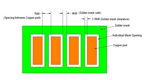
1. Solder Mask Clearance
Solder mask clearance refers to the distance between the edge of a pad and the opening in the solder mask. Adequate clearance is necessary to ensure that the solder mask does not encroach on the pad and interfere with the soldering process. The minimum solder mask clearance depends on the manufacturing capabilities of the PCB fabricator and the design requirements of the board.
| Pad Size (mm) | Minimum Solder Mask Clearance (mm) |
|---|---|
| ≤ 0.5 | 0.05 |
| 0.5 – 1.0 | 0.075 |
| 1.0 – 2.0 | 0.1 |
| > 2.0 | 0.15 |
2. Solder Mask Expansion
Solder mask expansion refers to the enlargement of the copper pads to compensate for the solder mask clearance. By expanding the pads, designers can ensure that the solder mask opening aligns properly with the pad and does not cause issues during soldering. The amount of solder mask expansion required depends on the minimum solder mask clearance and the tolerance of the manufacturing process.
3. Solder Mask Sliver
A solder mask sliver is a thin strip of solder mask between two adjacent pads or traces. If the gap between the pads is too small, the solder mask sliver may be too thin to provide adequate insulation and protection. To avoid this issue, designers should adhere to the minimum solder mask sliver width specified by the PCB fabricator.
4. Solder Mask Dams
Solder mask dams are small areas of solder mask placed between adjacent pads or traces to prevent solder bridging. These dams are especially useful in high-density designs where the risk of solder bridging is increased. By strategically placing solder mask dams, designers can improve the reliability and manufacturability of the PCB.

Solder Mask and High-Frequency PCB Design
In high-frequency PCB designs, solder mask plays a crucial role in maintaining signal integrity and reducing signal loss. At high frequencies, the dielectric properties of the solder mask material can significantly impact the characteristic impedance and propagation velocity of the signals.
Considerations for High-Frequency Solder Mask
-
Dielectric Constant (Dk): The dielectric constant of the solder mask material affects the characteristic impedance of the traces. A higher Dk value results in a lower characteristic impedance, which can cause impedance mismatches and signal reflections. For high-frequency designs, it is essential to choose a solder mask material with a low and stable Dk value.
-
Dissipation Factor (Df): The dissipation factor represents the energy loss in the solder mask material. A higher Df value leads to increased signal attenuation and reduced signal quality. In high-frequency applications, it is crucial to select a solder mask material with a low Df value to minimize signal loss.
-
Thickness: The thickness of the solder mask layer can also impact the characteristic impedance and signal propagation. Thicker solder mask layers can increase the effective dielectric constant, leading to lower characteristic impedance. In high-frequency designs, it is important to control the solder mask thickness and account for its effect on the trace geometry and impedance calculations.
Frequently Asked Questions (FAQ)
1. What is the difference between solder mask and silkscreen?
Solder mask is a protective layer applied to the copper traces of a PCB to prevent solder bridging and provide insulation. Silkscreen, on the other hand, is a printed layer of ink on top of the solder mask that contains component designators, logos, and other text for assembly and identification purposes.
2. Can solder mask be removed from a PCB?
Yes, solder mask can be removed from a PCB using various methods, such as mechanical abrasion, chemical etching, or laser ablation. However, removing the solder mask can expose the underlying copper traces to oxidation and contamination, compromising the integrity and reliability of the PCB.
3. What is the most common color for solder mask?
The most common colors for solder mask are green and blue. These colors provide good contrast with the copper traces and silkscreen markings, making the PCB easier to inspect and assemble. Other colors, such as red, yellow, black, and white, are also available for specific applications or aesthetic preferences.
4. How does solder mask affect the assembly process?
Solder mask plays a crucial role in the assembly process by preventing solder from bridging between adjacent pads and creating short circuits. The openings in the solder mask define the areas where solder can be applied, ensuring that components are properly soldered to the correct pads. Additionally, the silkscreen markings on top of the solder mask aid in the placement and orientation of components during assembly.
5. Can solder mask be applied to both sides of a PCB?
Yes, solder mask can be applied to both sides of a PCB, depending on the design requirements. In double-sided PCB designs, solder mask is typically applied to both the top and bottom layers to provide protection and insulation for the copper traces on both sides. In multi-layer PCBs, solder mask is usually only applied to the outer layers, as the inner layers are protected by the laminated structure of the board.
Conclusion
Solder mask is an essential component of modern PCB design, providing numerous benefits, such as preventing solder bridges and short circuits, protecting against oxidation and contamination, improving durability and insulation, and enhancing the aesthetic appeal of the board. When designing a PCB with solder mask, it is crucial to consider factors such as solder mask clearance, expansion, sliver, and dams to ensure proper functionality and manufacturability.
In high-frequency PCB designs, the choice of solder mask material and its properties, such as dielectric constant, dissipation factor, and thickness, can significantly impact signal integrity and performance. By carefully selecting the appropriate solder mask material and accounting for its effects on trace geometry and impedance, designers can optimize their high-frequency PCBs for maximum reliability and signal quality.
As PCB technology continues to advance, the role of solder mask in enabling more complex and compact designs will only become more critical. By understanding the functions, benefits, and design considerations of solder mask, PCB designers and manufacturers can create more reliable, durable, and high-performance electronic devices to meet the ever-growing demands of the industry.
Leave a Reply