Introduction to PCB Solder Mask
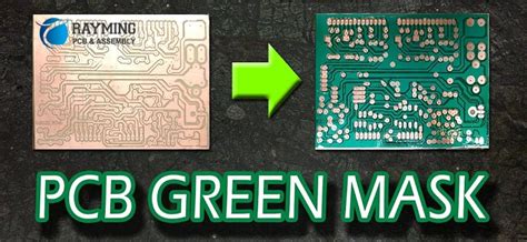
Solder mask, also known as solder resist or solder stop, is a vital component in the manufacturing of printed circuit boards (PCBs). It is a thin, protective layer applied to the copper traces and pads on a PCB, leaving only the areas that need to be soldered exposed. The primary purpose of solder mask is to prevent solder bridging and short circuits, while also protecting the copper from oxidation and contamination.
Key Functions of Solder Mask on PCBs
- Insulation: Solder mask acts as an insulating layer, preventing accidental electrical connections between adjacent traces and pads.
- Protection: It protects the copper traces from oxidation, corrosion, and mechanical damage during handling and assembly.
- Aesthetics: Solder mask gives PCBs a professional appearance and can be used to add branding or text to the board.
Types of Solder Mask
There are two main types of solder mask used in PCB manufacturing:
1. Liquid Photoimageable Solder Mask (LPSM)
LPSM is the most common type of solder mask used in the industry. It is applied as a liquid coating and then exposed to UV light through a photomask to cure and harden the desired areas.
2. Dry Film Solder Mask (DFSM)
DFSM is a solid film that is laminated onto the PCB surface using heat and pressure. It is then exposed to UV light through a photomask, similar to LPSM. DFSM is less common than LPSM but offers some advantages, such as better edge definition and improved adhesion.

Solder Mask Application Process
The process of applying solder mask to a PCB involves several steps:
1. Cleaning and Preparation
Before applying solder mask, the PCB surface must be thoroughly cleaned to remove any contaminants, such as dirt, grease, or oxidation. This is typically done using a chemical cleaning process, followed by a rinse with deionized water and drying.
2. Solder Mask Application
Liquid Photoimageable Solder Mask (LPSM)
- The liquid solder mask is applied to the PCB surface using a screen printing, spraying, or curtain coating method.
- The coated PCB is then prebaked to partially cure the solder mask and remove any solvents.
Dry Film Solder Mask (DFSM)
- The dry film is laminated onto the PCB surface using heat and pressure.
- The laminated PCB is then allowed to cool and stabilize.
3. Exposure and Development
- The coated or laminated PCB is aligned with a photomask, which contains the desired solder mask pattern.
- The PCB is exposed to UV light through the photomask, causing the exposed areas of the solder mask to cure and harden.
- The unexposed areas of the solder mask are then removed using a chemical developer solution, revealing the copper traces and pads that need to be soldered.
4. Curing and Finishing
- After development, the PCB is post-baked to fully cure the remaining solder mask and improve its mechanical and chemical properties.
- The PCB may then undergo additional finishing steps, such as surface finish application (e.g., HASL, ENIG, or OSP) and final inspection.

Solder Mask Properties and Specifications
When selecting a solder mask for a specific application, several properties and specifications must be considered:
1. Dielectric Strength
Dielectric strength is the maximum electric field that the solder mask can withstand before breaking down and allowing current to flow. A higher dielectric strength provides better insulation and protection against voltage spikes.
2. Dielectric Constant
The dielectric constant is a measure of the solder mask’s ability to store electric charge. A lower dielectric constant is desirable for high-frequency applications, as it reduces signal loss and distortion.
3. Surface Resistance
Surface resistance is the resistance to current flow across the surface of the solder mask. A higher surface resistance helps prevent leakage currents and improves insulation.
4. Flammability Rating
The flammability rating indicates the solder mask’s resistance to ignition and flame spread. Common ratings include UL 94V-0, which is the highest rating for PCB materials.
5. Thermal Shock Resistance
Thermal shock resistance is the ability of the solder mask to withstand rapid changes in temperature without cracking or delaminating. This is important for applications that expose the PCB to extreme temperature fluctuations.
6. Adhesion Strength
Adhesion strength is a measure of how well the solder mask adheres to the PCB surface. Good adhesion is critical for long-term reliability and protection against delamination.

Solder Mask Color Options
Solder mask is available in a variety of colors, with green being the most common. Other popular color options include:
- Blue
- Red
- Yellow
- Black
- White
The choice of color is often a matter of preference or branding, but it can also serve functional purposes. For example, white solder mask is sometimes used for LED lighting applications to improve light reflection and distribution.
Solder Mask Thickness and Coverage
The thickness of the solder mask layer can vary depending on the application and the specific solder mask material used. Typical thicknesses range from 0.5 mil (0.0127 mm) to 2 mil (0.0508 mm).
Solder mask coverage is another important consideration. The solder mask should cover all areas of the PCB except for the pads and other features that need to be soldered. The size and shape of the openings in the solder mask can affect the ease and quality of soldering.
Solder Mask Design Considerations
When designing a PCB with solder mask, several factors should be taken into account:
1. Pad and Trace Spacing
The spacing between pads and traces must be sufficient to allow for proper solder mask coverage and prevent bridging. Minimum spacing requirements may vary depending on the solder mask material and application method.
2. Solder Mask Expansion
During the curing process, solder mask may expand slightly. This expansion must be accounted for in the design to ensure that the final dimensions of the pads and openings are within tolerance.
3. Solder Mask Registration
Proper alignment between the solder mask and the underlying copper features is critical for ensuring reliable electrical connections. The design should include registration marks or fiducials to aid in aligning the solder mask during the application process.
4. Solder Mask Sliver Prevention
Solder mask slivers are thin strips of solder mask that can occur between closely spaced pads or traces. These slivers can be difficult to remove during development and may cause issues with soldering. The design should incorporate strategies to minimize or eliminate solder mask slivers, such as adding teardrops or adjusting pad geometry.
Frequently Asked Questions (FAQ)
1. What is the difference between solder mask and conformal coating?
Solder mask is applied to the PCB before assembly and is designed to prevent solder bridging and protect the copper features. Conformal coating is applied after assembly and provides additional protection against moisture, dust, and other environmental factors.
2. Can solder mask be removed after application?
Yes, solder mask can be removed using specialized stripping solutions or mechanical abrasion. However, removing solder mask can be difficult and may damage the underlying copper features if not done carefully.
3. How does solder mask affect PCB impedance?
Solder mask has a higher dielectric constant than air, which can affect the impedance of the PCB traces. This effect must be accounted for in the design, especially for high-frequency or impedance-controlled applications.
4. Can solder mask be applied selectively to certain areas of the PCB?
Yes, selective solder mask application is possible using specialized techniques such as spot masking or Laser Direct Imaging (LDI). This can be useful for applications that require exposed copper features in specific areas of the PCB.
5. How does solder mask affect the assembly process?
Solder mask can impact the assembly process in several ways. It can affect the wetting and spreading of solder, as well as the placement and alignment of components. Proper solder mask design and application are critical for ensuring a smooth and reliable assembly process.
Conclusion
Solder mask is an essential component of modern PCB manufacturing, providing critical protection and insulation for the copper features on the board. The application of solder mask involves a multi-step process of cleaning, coating, exposing, and curing, which must be carefully controlled to achieve the desired properties and performance.
When designing a PCB with solder mask, engineers must consider factors such as pad spacing, expansion, registration, and sliver prevention to ensure a reliable and manufacturable board. The choice of solder mask material, color, and thickness can also impact the performance and aesthetics of the final product.
By understanding the principles and best practices of solder mask application, PCB designers and manufacturers can create high-quality, reliable circuits that meet the demands of a wide range of applications, from consumer electronics to aerospace and beyond.
| Solder Mask Property | Typical Value Range |
|---|---|
| Dielectric Strength | 500 – 1500 V/mil |
| Dielectric Constant | 3.0 – 5.0 |
| Surface Resistance | 10^12 – 10^14 ohms |
| Flammability Rating | UL 94V-0 |
| Thermal Shock Resistance | -65°C to 125°C |
| Adhesion Strength | 4 – 5 lbs/in (peel strength) |
| Thickness | 0.5 – 2 mil (0.0127 – 0.0508 mm) |
Leave a Reply